SBVS087M June   2008  – June 2018 TPS735

PRODUCTION DATA.  

  1. Features
  2. Applications
  3. Description
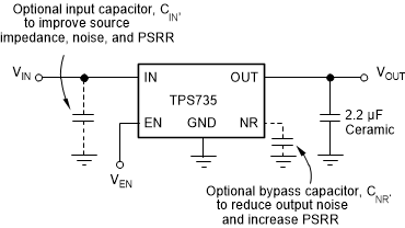
    1.     Typical Application
  4. Revision History
    1.     Pin Configuration and Functions
      1.      Pin Functions
  5. Specifications
    1. 5.1 Absolute Maximum Ratings
    2. 5.2 ESD Ratings
    3. 5.3 Recommended Operating Conditions
    4. 5.4 Thermal Information
    5. 5.5 Electrical Characteristics
    6. 5.6 Typical Characteristics
  6. Detailed Description
    1. 6.1 Overview
    2. 6.2 Functional Block Diagrams
    3. 6.3 Feature Description
      1. 6.3.1 Internal Current Limit
      2. 6.3.2 Shutdown
      3. 6.3.3 Dropout Voltage
      4. 6.3.4 Start-Up and Noise Reduction Capacitor
      5. 6.3.5 Transient Response
      6. 6.3.6 Undervoltage Lockout
      7. 6.3.7 Minimum Load
      8. 6.3.8 Thermal Protection
    4. 6.4 Device Functional Modes
      1. 6.4.1 Normal Operation
      2. 6.4.2 Dropout Operation
      3. 6.4.3 Disabled
  7. Application and Implementation
    1. 7.1 Application Information
    2. 7.2 Typical Applications
      1. 7.2.1 Design Requirements
        1. 7.2.1.1 Input and Output Capacitor Requirements
        2. 7.2.1.2 Feed-Forward Capacitor Requirements
      2. 7.2.2 Detailed Design Procedure
        1. 7.2.2.1 Output Noise
      3. 7.2.3 Application Curves
  8. Power Supply Recommendations
  9. Layout
    1. 9.1 Layout Guidelines
      1. 9.1.1 Board Layout Recommendations to Improve PSRR and Noise Performance
    2. 9.2 Layout Example
    3. 9.3 Power Dissipation
    4. 9.4 Estimating Junction Temperature
    5. 9.5 Package Mounting
  10. 10Device and Documentation Support
    1. 10.1 Device Support
      1. 10.1.1 Development Support
        1. 10.1.1.1 Evaluation Modules
      2. 10.1.2 Device Nomenclature
    2. 10.2 Documentation Support
      1. 10.2.1 Related Documentation
    3. 10.3 Trademarks
    4. 10.4 Electrostatic Discharge Caution
    5. 10.5 Glossary
  11. 11Mechanical, Packaging, and Orderable Information

Package Options

Mechanical Data (Package|Pins)
Thermal pad, mechanical data (Package|Pins)
Orderable Information

Description

The TPS735 low-dropout (LDO), low-power linear regulator offers excellent AC performance with very low ground current. High power-supply rejection ratio (PSRR), low noise, fast start-up, and excellent line and load transient responses are provided while consuming a very low 45-μA (typical) ground current.

The TPS735 device is stable with ceramic capacitors and uses an advanced BiCMOS fabrication process to yield a typical dropout voltage of 280 mV at 500-mA output. The TPS735 device uses a precision voltage reference and feedback loop to achieve overall accuracy of 2% (VOUT> 2.2 V) over all load, line, process, and temperature variations. This device is fully specified from TJ = –40°C to +125°C and is offered in a low-profile, 3 mm × 3 mm SON-8 package and a 2 mm × 2 mm WSON-6 package.

Device Information(1)

PART NUMBER PACKAGE BODY SIZE (NOM)
TPS735 WSON (6) 2.00 mm × 2.00 mm
SON (8) 3.00 mm × 3.00 mm
  1. For all available packages, see the orderable addendum at the end of the data sheet.

Typical Application
TPS735 alt_sbvs087.gif