SBVS064N December   2005  – November 2016 TPS74201

PRODUCTION DATA.  

  1. Features
  2. Applications
  3. Description
  4. Revision History
  5. Pin Configuration and Functions
  6. Specifications
    1. 6.1 Absolute Maximum Ratings
    2. 6.2 ESD Ratings
    3. 6.3 Recommended Operating Conditions
    4. 6.4 Thermal Information
    5. 6.5 Electrical Characteristics
    6. 6.6 Typical Characteristics
  7. Detailed Description
    1. 7.1 Overview
    2. 7.2 Functional Block Diagram
    3. 7.3 Feature Description
      1. 7.3.1 Enable and Shutdown
      2. 7.3.2 Power-Good (VQFN Packages Only)
      3. 7.3.3 Internal Current Limit
    4. 7.4 Device Functional Modes
      1. 7.4.1 Normal Operation
      2. 7.4.2 Dropout Operation
      3. 7.4.3 Disabled
  8. Application and Implementation
    1. 8.1 Application Information
      1. 8.1.1 Input, Output, and Bias Capacitor Requirements
      2. 8.1.2 Transient Response
      3. 8.1.3 Dropout Voltage
      4. 8.1.4 Output Noise
      5. 8.1.5 Programmable Soft-Start
      6. 8.1.6 Sequencing Requirements
    2. 8.2 Typical Applications
      1. 8.2.1 Design Requirements
      2. 8.2.2 Detailed Design Procedure
      3. 8.2.3 Application Curves
  9. Power Supply Recommendations
  10. 10Layout
    1. 10.1 Layout Guidelines
    2. 10.2 Layout Example
    3. 10.3 Thermal Protection
    4. 10.4 Thermal Considerations
  11. 11Device and Documentation Support
    1. 11.1 Device Support
      1. 11.1.1 Development Support
        1. 11.1.1.1 Evaluation Modules
        2. 11.1.1.2 Spice Models
    2. 11.2 Documentation Support
      1. 11.2.1 Related Documentation
    3. 11.3 Receiving Notification of Documentation Updates
    4. 11.4 Community Resources
    5. 11.5 Trademarks
    6. 11.6 Electrostatic Discharge Caution
    7. 11.7 Glossary
  12. 12Mechanical, Packaging, and Orderable Information

Package Options

Mechanical Data (Package|Pins)
Thermal pad, mechanical data (Package|Pins)
Orderable Information

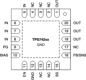
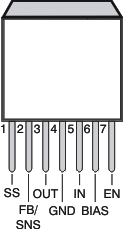
Pin Configuration and Functions

RGW, RGR Packages
20-Pin VQFN with Exposed Thermal Pad
Top View
TPS74201 po_rgw_bvs064.gif
KTW Package
7-Pin DDPAK/TO-263
Top View
TPS74201 po_ktw_bvs064.gif

Pin Functions

PIN I/O DESCRIPTION
NAME KTW (DDPAK/
TO-263)
RGW, RGR (VQFN)
BIAS 6 10 I Bias input voltage for error amplifier, reference, and internal control circuits.
EN 7 11 I Enable pin. Driving this pin high enables the regulator. Driving this pin low puts the regulator into shutdown mode. This pin must not be left floating.
FB 2 16 I This pin is the feedback connection to the center tap of an external resistor divider network that sets the output voltage. This pin must not be left floating. (Adjustable version only.)
GND 4 12 Ground
IN 5 5,6,7,8 I Unregulated input to the device.
NC 2, 3,4, 13,14,17 O No connection. This pin can be left floating or connected to GND to allow better thermal contact to the top-side plane.
OUT 3 1, 18, 19, 20 O Regulated output voltage. No capacitor is required on this pin for stability.
PAD/TAB Solder to the ground plane for increased thermal performance.
PG 9 O Power-Good (PG) is an open-drain, active-high output that indicates the status of VOUT. When VOUT exceeds the PG trip threshold, the PG pin goes into a high-impedance state. When VOUT is below this threshold the pin is driven to a low-impedance state. Connect a pullup resistor from 10 kΩ to 1 MΩ from this pin to a supply up to 5.5 V. The supply can be higher than the input voltage. Alternatively, the PG pin can be left floating if output monitoring is not necessary.
SNS 2 16 I This pin is the sense connection to the load device. This pin must be connected to VOUT and must not be left floating. (Fixed versions only.)
SS 1 15 Soft-Start pin. A capacitor connected on this pin to ground sets the start-up time. If this pin is left floating, the regulator output soft-start ramp time is typically 100 μs.