SBVS135J June   2010  – January 2018 TPS7A80

PRODUCTION DATA.  

  1. Features
  2. Applications
  3. Description
    1.     Device Images
      1.      Typical Application Diagram
  4. Revision History
  5. Pin Configuration and Functions
    1.     Pin Functions
  6. Specifications
    1. 6.1 Absolute Maximum Ratings
    2. 6.2 ESD Ratings
    3. 6.3 Recommended Operating Conditions
    4. 6.4 Thermal Information
    5. 6.5 Electrical Characteristics
    6. 6.6 Typical Characteristics
  7. Detailed Description
    1. 7.1 Overview
    2. 7.2 Functional Block Diagram
    3. 7.3 Feature Description
      1. 7.3.1 Internal Current Limit
      2. 7.3.2 Shutdown
      3. 7.3.3 Start-Up
      4. 7.3.4 Undervoltage Lockout (UVLO)
    4. 7.4 Device Functional Modes
  8. Application and Implementation
    1. 8.1 Application Information
    2. 8.2 Typical Application
      1. 8.2.1 Design Requirements
        1. 8.2.1.1 Dropout Voltage
        2. 8.2.1.2 Minimum Load
        3. 8.2.1.3 Input and Output Capacitor Requirements
        4. 8.2.1.4 Transient Response
      2. 8.2.2 Detailed Design Procedure
        1. 8.2.2.1 Output Noise
      3. 8.2.3 Application Curve
  9. Power Supply Recommendations
  10. 10Layout
    1. 10.1 Layout Guidelines
      1. 10.1.1 Board Layout Recommendations to Improve PSRR and Noise Performance
      2. 10.1.2 Thermal Considerations
      3. 10.1.3 Power Dissipation
      4. 10.1.4 Estimating Junction Temperature
    2. 10.2 Layout Example
  11. 11Device and Documentation Support
    1. 11.1 Documentation Support
      1. 11.1.1 Related Documentation
    2. 11.2 Receiving Notification of Documentation Updates
    3. 11.3 Community Resources
    4. 11.4 Trademarks
    5. 11.5 Electrostatic Discharge Caution
    6. 11.6 Glossary
  12. 12Mechanical, Packaging, and Orderable Information

Package Options

Mechanical Data (Package|Pins)
Thermal pad, mechanical data (Package|Pins)
Orderable Information

Typical Characteristics

At VOUT(TYP) = 3.3 V, VIN = VOUT(TYP) + 0.5 V or 2.2 V (whichever is greater), IOUT = 100 mA, VEN = VIN, CIN = 1 μF,
COUT = 4.7 μF, and CNR = 0.01 μF, all temperature values refer to TJ (unless otherwise noted).
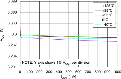
TPS7A80 tc_load_reg_bvs135.gif
Figure 1. Load Regulation
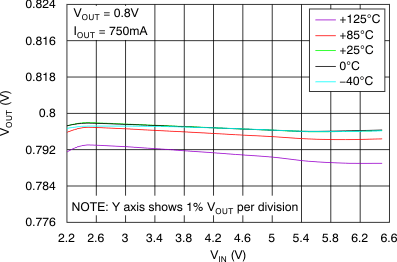
TPS7A80 tc_line_reg_bvs135.gif
Figure 3. Line Regulation
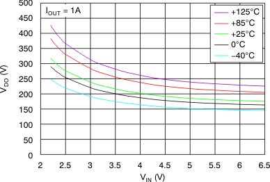
TPS7A80 tc_vdo-vin_1a_bvs135.gif
Figure 5. Dropout Voltage vs Input Voltage
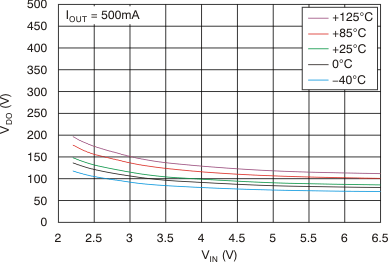
TPS7A80 tc_vdo-vin_500ma_bvs135.gif
Figure 7. Dropout Voltage vs Input Voltage
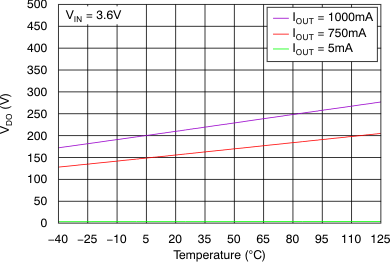
TPS7A80 tc_vdo-tmp_bvs135.gif
Figure 9. Dropout Voltage vs Temperature
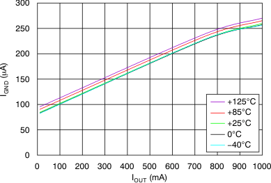
TPS7A80 tc_ignd-iout_bvs135.gif
Figure 11. Ground Pin Current vs Load Current
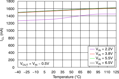
TPS7A80 tc_ilim-tmp_bvs135.gif
Figure 13. Current Limit vs Temperature
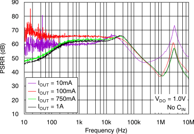
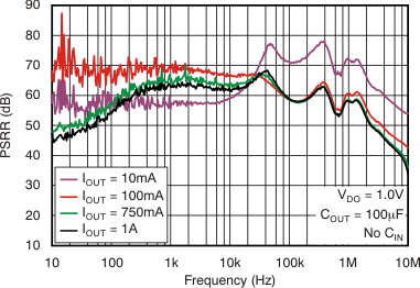
TPS7A80 tc_psrr-frq_1v_bvs135.gif
Figure 15. Power-Supply Ripple Rejection vs Frequency
TPS7A80 tc_psrr-frq_1v_22uf_bvs135.gif
Figure 17. Power-Supply Ripple Rejection vs Frequency
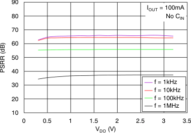
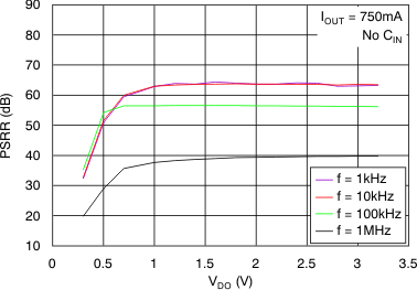
TPS7A80 tc_psrr-vdo_100ma_bvs135.gif
Figure 19. Power-Supply Ripple Rejection
vs Dropout Voltage
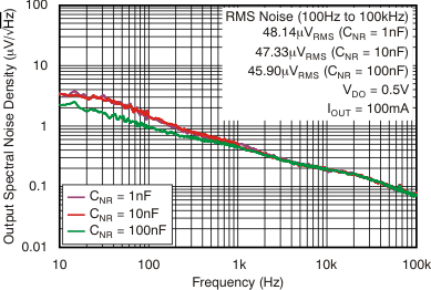
TPS7A80 tc_noise-frq_4795_bvs135.gif
Figure 21. Output Spectral Noise Density
vs Frequency
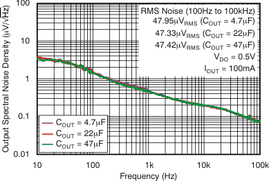
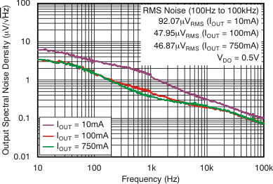
TPS7A80 tc_noise-frq_9207_bvs135.gif
Figure 23. Output Spectral Noise Density
vs Frequency
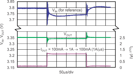
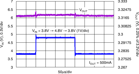
TPS7A80 tc_line_trans_bvs135.gif
Figure 25. Line Transient Response
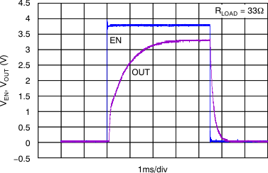
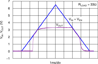
TPS7A80 tc_en_pulse_bvs135.gif
Figure 27. Enable Pulse Response
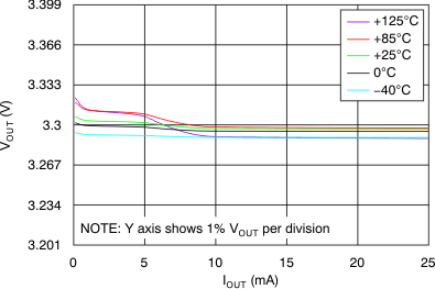
TPS7A80 tc_load_reg_light_bvs135.gif
Figure 2. Load Regulation Under Light Loads
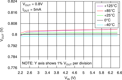
TPS7A80 tc_line_reg_light_bvs135.gif
Figure 4. Line Regulation Under Light Loads
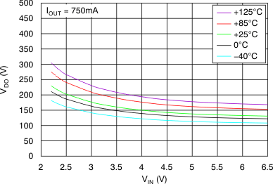
TPS7A80 tc_vdo-vin_750ma_bvs135.gif
Figure 6. Dropout Voltage vs Input Voltage
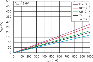
TPS7A80 tc_vdo-iout_bvs135.gif
Figure 8. Dropout Voltage vs Load Current
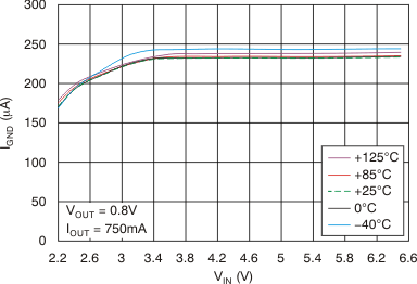
TPS7A80 tc_ignd-vin_bvs135.gif
Figure 10. Ground Pin Current vs Input Voltage
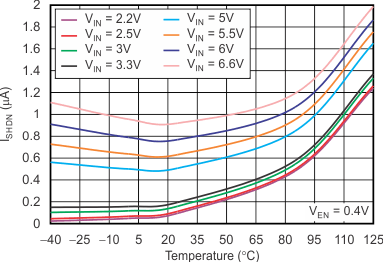
TPS7A80 tc_ishdn-tmp_bvs135.gif
Figure 12. Shutdown Current vs Temperature
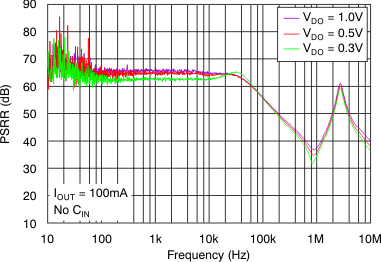
TPS7A80 tc_psrr-frq_100ma_bvs135.gif
Figure 14. Power-Supply Ripple Rejection vs Frequency
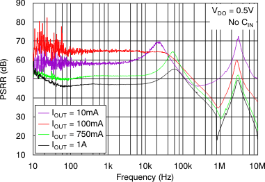
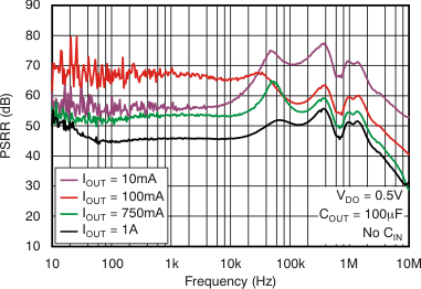
TPS7A80 tc_psrr-frq_05v_bvs135.gif
Figure 16. Power-Supply Ripple Rejection vs Frequency
TPS7A80 tc_psrr-frq_05v_22uf_bvs135.gif
Figure 18. Power-Supply Ripple Rejection vs Frequency