SBVS324A June   2017  – June 2020 TPS7A90

PRODUCTION DATA.  

  1. Features
  2. Applications
  3. Description
    1.     Device Images
      1.      Typical Application Circuit
      2.      Typical Application Diagram
  4. Revision History
  5. Pin Configuration and Functions
    1.     Pin Functions
  6. Specifications
    1. 6.1 Absolute Maximum Ratings
    2. 6.2 ESD Ratings
    3. 6.3 Recommended Operating Conditions
    4. 6.4 Thermal Information
    5. 6.5 Electrical Characteristics
    6. 6.6 Typical Characteristics
  7. Detailed Description
    1. 7.1 Overview
    2. 7.2 Functional Block Diagram
    3. 7.3 Feature Description
      1. 7.3.1 Output Enable
      2. 7.3.2 Dropout Voltage (VDO)
      3. 7.3.3 Output Voltage Accuracy
      4. 7.3.4 High Power-Supply Rejection Ratio (PSRR)
      5. 7.3.5 Low Output Noise
      6. 7.3.6 Output Soft-Start Control
      7. 7.3.7 Power-Good Function
      8. 7.3.8 Internal Protection Circuitry
        1. 7.3.8.1 Undervoltage Lockout (UVLO)
        2. 7.3.8.2 Internal Current Limit (ICL)
        3. 7.3.8.3 Thermal Protection
    4. 7.4 Device Functional Modes
      1. 7.4.1 Normal Operation
      2. 7.4.2 Dropout Operation
      3. 7.4.3 Disabled
  8. Application and Implementation
    1. 8.1 Application Information
      1. 8.1.1 Adjustable Output
      2. 8.1.2 Start-Up
        1. 8.1.2.1 Enable (EN) and Undervoltage Lockout (UVLO)
        2. 8.1.2.2 Noise-Reduction and Soft-Start Capacitor (CNR/SS)
          1. 8.1.2.2.1 Noise Reduction
          2. 8.1.2.2.2 Soft-Start and In-Rush Current
      3. 8.1.3 Capacitor Recommendation
        1. 8.1.3.1 Input and Output Capacitor Requirements (CIN and COUT)
          1. 8.1.3.1.1 Load-Step Transient Response
        2. 8.1.3.2 Feed-Forward Capacitor (CFF)
      4. 8.1.4 Power Dissipation (PD)
      5. 8.1.5 Estimating Junction Temperature
    2. 8.2 Typical Application
      1. 8.2.1 Design Requirements
      2. 8.2.2 Detailed Design Procedure
      3. 8.2.3 Application Curves
  9. Power Supply Recommendations
  10. 10Layout
    1. 10.1 Layout Guidelines
      1. 10.1.1 Board Layout
    2. 10.2 Layout Example
  11. 11Device and Documentation Support
    1. 11.1 Device Support
      1. 11.1.1 Development Support
        1. 11.1.1.1 Evaluation Modules
        2. 11.1.1.2 SPICE Models
      2. 11.1.2 Device Nomenclature
    2. 11.2 Documentation Support
      1. 11.2.1 Related Documentation
    3. 11.3 Receiving Notification of Documentation Updates
    4. 11.4 Support Resources
    5. 11.5 Trademarks
    6. 11.6 Electrostatic Discharge Caution
    7. 11.7 Glossary
  12. 12Mechanical, Packaging, and Orderable Information

Package Options

Mechanical Data (Package|Pins)
Thermal pad, mechanical data (Package|Pins)
Orderable Information

Typical Characteristics

at TJ = 25°C, 1.4 V ≤ VIN ≤ 6.5 V, VIN ≥ VOUT(NOM) + 0.3 V, VOUT = 0.8 V, SS_CTRL = GND, IOUT = 5 mA, VEN = 1.1 V, COUT = 10 μF, CNR/SS = CFF = 0 nF, PG pin pulled up to VOUT with 100 kΩ, and SS_CTRL = GND (unless otherwise noted)
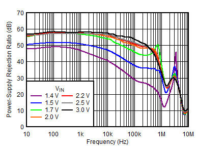
TPS7A90 Figure1-PSRRvsFreqvsVin.gif
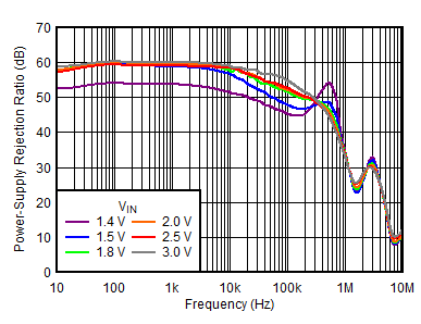
VOUT = 0.8 V, IOUT = 500 mA, COUT = 10 µF,
CNR/SS = CFF = 10 nF
Figure 1. PSRR vs Frequency and Input Voltage
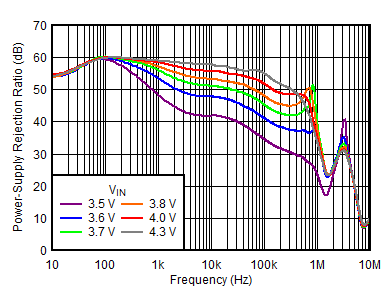
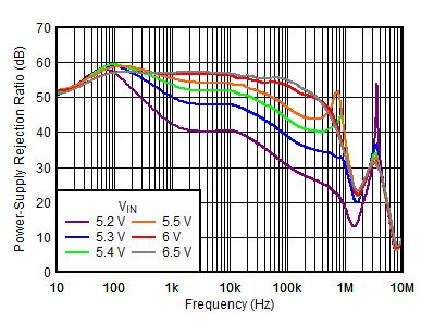
TPS7A90 Figure3-PSRRvsFreqvsVinVout=3.3V.gif
VOUT = 3.3 V, IOUT = 500 mA, COUT = 10 µF,
CNR/SS = CFF = 10 nF
Figure 3. PSRR vs Frequency and Input Voltage
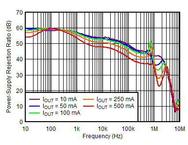
TPS7A90 Figure5-PSRRvsFreqvsIoutVout=1.2V.gif
VOUT = 1.2 V, VIN = VEN = 1.5 V, COUT = 10 µF,
CNR/SS = CFF = 10 nF
Figure 5. PSRR vs Frequency and Output Current
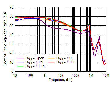
TPS7A90 Figure7-PSRRvsFreqvsCnrVout=1.2V.gif
VOUT = 1.2 V, VIN = VEN = 1.7 V, IOUT = 500 mA, COUT = 10 µF,
CFF = 10 nF
Figure 7. PSRR vs Frequency and CNR/SS
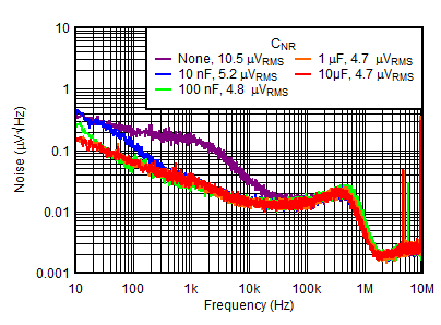
TPS7A90 Figure9-NoisevsFreqvsCnr.gif
VIN = 2.2 V, VOUT = 1.2 V, IOUT = 500 mA, CIN = COUT = 10 µF,
CFF = 10 nF, VRMS BW = 10 Hz to 100 kHz
Figure 9. Spectral Noise Density vs Frequency and CNR/SS
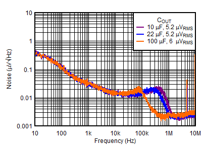
TPS7A90 Figure11-NoisevsFreqvsCout.gif
VIN = 2.2 V, VOUT = 1.2 V, IOUT = 500 mA, CIN = 10 µF,
CNR/SS = CFF = 10 nF, VRMS BW = 10 Hz to 100 kHz
Figure 11. Spectral Noise Density vs Frequency and COUT
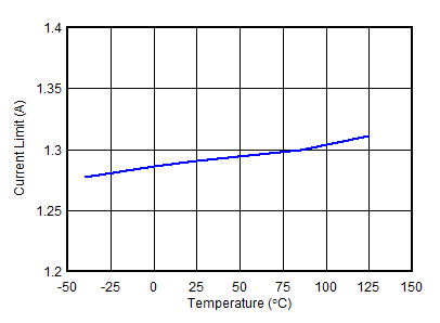
TPS7A90 D013-SBVS324-01.gif
VIN = 1.4 V, VOUT = 0.8 V
Figure 13. Current Limit vs Temperature
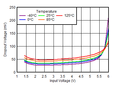
TPS7A90 D015-SBVS324-01.gif
IOUT = 500 mA
Figure 15. Dropout Voltage vs Input Voltage
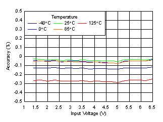
TPS7A90 tc_Vout_Vin.gif
IOUT = 50 mA
Figure 17. Line Regulation
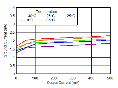
TPS7A90 D019-SBVS324-01.gif
VIN = 1.4 V
Figure 19. Ground Current vs Output Current
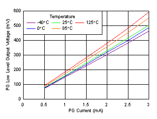
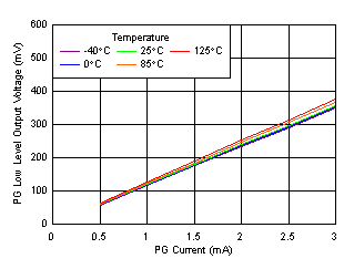
TPS7A90 tc_Vol_Ipg_1.5V.gif
Figure 21. PG Low Level Voltage vs PG Current
(VIN = 1.4 V)
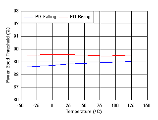
TPS7A90 tc_PG_Temp.gif
Figure 23. PG Threshold vs Temperature
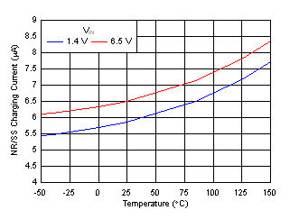
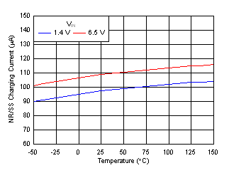
TPS7A90 tc_Inr_CNTRL_GND.gif
Figure 25. Soft-Start Current vs Temperature
(SS_CTRL = GND)
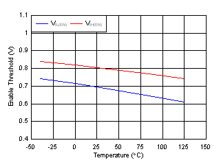
TPS7A90 tc_Ven_temp.gif
Figure 27. Enable Threshold vs Temperature
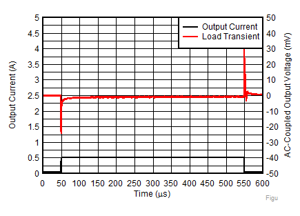
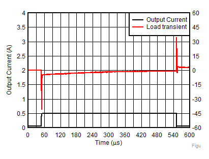
TPS7A90 Figure29-LoadTransient0.8Vout.gif
VIN = 1.4 V, IOUT = 50 mA to 500 mA to 50 mA at 1 A/µs,
COUT = 10 µF, VPG = VOUT
Figure 29. Load Transient Response (VOUT = 0.8 V)
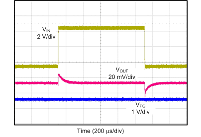
TPS7A90 tc_line_trans_sbvs282.gif
VIN = 1.4 V to 6.5 V to 1.4 V at 2 V/µs, VOUT = 0.8 V,
IOUT = 500 mA, CNR/SS = CFF = 10 nF, VPG = VOUT
Figure 31. Line Transient
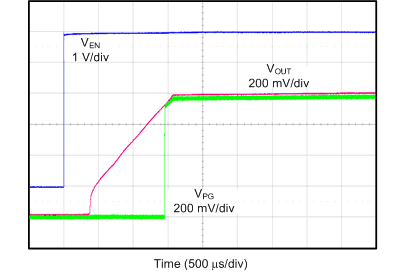
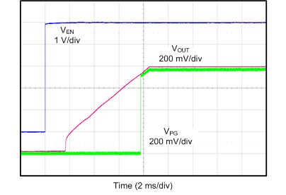
TPS7A90 tc_startup_01_GND_sbvs282.gif
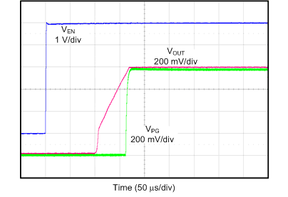
VIN = 1.4 V, VPG = VOUT
Figure 33. Start-Up (SS_CTRL = GND, CNR/SS = 10 nF)
TPS7A90 tc_startup_1_VIN_sbvs282.gif
VIN = 1.4 V, VPG = VOUT
Figure 35. Start-Up (SS_CTRL = VIN, CNR/SS = 1 µF)
TPS7A90 Figure2-PSRRvsFreqvsVinVout=1.2V.gif
VOUT = 1.2 V, IOUT = 500 mA, COUT = 10 µF,
CNR/SS = CFF = 10 nF
Figure 2. PSRR vs Frequency and Input Voltage
TPS7A90 Figure4-PSRRvsFreqvsVinVout=5.0V.gif
VOUT = 5 V, IOUT = 500 mA, COUT = 10 µF,
CNR/SS = CFF = 10 nF
Figure 4. PSRR vs Frequency and Input Voltage
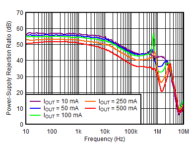
TPS7A90 Figure6-PSRRvsFreqvsIoutVout=3.3V.gif
VOUT = 3.3 V, VIN = VEN = 3.6 V, COUT = 10 µF,
CNR/SS = CFF = 10 nF
Figure 6. PSRR vs Frequency and Output Current
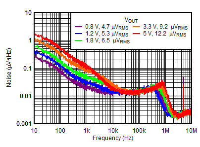
TPS7A90 Figure8-NoisevsFreqvsVout.gif
VIN = VOUT + 1.0 V, IOUT = 500 mA, CIN = COUT = 10 µF,
CNR/SS = CFF = 10 nF, VRMS BW = 10 Hz to 100 kHz
Figure 8. Spectral Noise Density vs Frequency and
Output Voltage
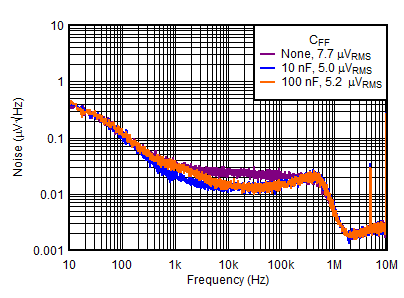
TPS7A90 Figure10-NoisevsFreqvsCff.gif
VIN = 2.2 V, VOUT = 1.2 V, IOUT = 500 mA, CIN = COUT = 10 µF, CNR/SS = 10 nF, VRMS BW = 10 Hz to 100 kHz
Figure 10. Spectral Noise Density vs Frequency and CFF
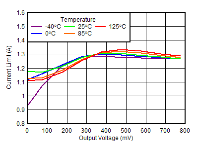
TPS7A90 D012SBVS32401.gif
VIN = 1.4 V, VOUT = 0.8 V
Figure 12. Current Limit Foldback
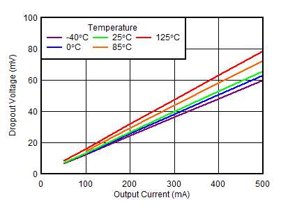
TPS7A90 D014-SBVS324-01.gif
VIN = 5.5 V
Figure 14. Dropout Voltage vs Output Current
TPS7A90 D016-SBVS324-01.gif
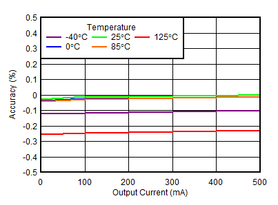
VIN = 1.4 V
Figure 16. Load Regulation
TPS7A90 tc_Isht_Vin.gif
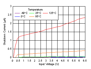
VEN = 0.4 V
Figure 18. Shutdown Current vs Input Voltage
TPS7A90 tc_Ignd_Vin.gif
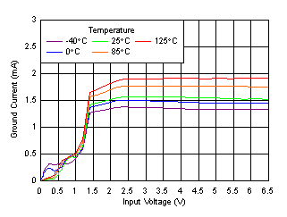
Figure 20. Ground Current vs Input Voltage
TPS7A90 tc_Vol_Ipg_6.5V.gif
Figure 22. PG Low Level Voltage vs PG Current
(VIN = 6.5 V)
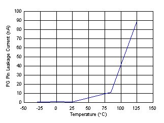
TPS7A90 tc_PGlkg_Temp.gif
VIN = VPG = 6.5 V
Figure 24. PG Leakage Current vs Temperature
TPS7A90 tc_Inr_CNTRL_Vin.gif
Figure 26. Soft-Start Current vs Temperature
(SS_CTRL = VIN)
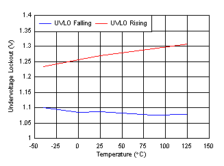
TPS7A90 tc_UVLO_temp.gif
Figure 28. Input UVLO Threshold vs Temperature
TPS7A90 Figure30-LoadTransient5.0Vout.gif
VIN = 5.5 V, IOUT = 50 mA to 500 mA to 50 mA at 1 A/µs,
COUT = 10 µF, VPG = VOUT
Figure 30. Load Transient Response (VOUT = 5.0 V)
TPS7A90 tc_startup_0_GNDr_sbvs282.gif
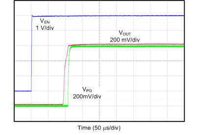
VIN = 1.4 V, VPG = VOUT
Figure 32. Start-Up (SS_CTRL = GND, CNR/SS = 0 nF)
TPS7A90 tc_startup_01_VIN_sbvs282.gif
VIN = 1.4 V, VPG = VOUT
Figure 34. Start-Up (SS_CTRL = VIN, CNR/SS = 10 nF)