SLVSBK3A December 2012 – September 2015 TPS92690
PRODUCTION DATA.
- 1 Features
- 2 Applications
- 3 Description
- 4 Revision History
- 5 Pin Configuration and Functions
- 6 Specifications
-
7 Detailed Description
- 7.1 Overview
- 7.2 Functional Block Diagram
- 7.3
Feature Description
- 7.3.1 Current Regulators
- 7.3.2 Peak Current Mode Control
- 7.3.3 Switching Frequency and Synchronization
- 7.3.4 Current Sense and Current Limit
- 7.3.5 Average LED Current
- 7.3.6 Precision Reference (VREF)
- 7.3.7 Low-Level Analog Dimming
- 7.3.8 Soft-Start and Shutdown
- 7.3.9 VCC Regulator and Start-Up
- 7.3.10 Overvoltage Protection (OVP)
- 7.3.11 Input Undervoltage Lockout (UVLO)
- 7.3.12 PWM Dimming
- 7.3.13 Control Loop Compensation
- 7.3.14 Thermal Shutdown
- 7.4 Device Functional Modes
-
8 Application and Implementation
- 8.1 Application Information
- 8.2
Typical Applications
- 8.2.1
Basic Topology Schematics
- 8.2.1.1 Design Requirements
- 8.2.1.2
Detailed Design Procedure
- 8.2.1.2.1 Operating Point
- 8.2.1.2.2 Switching Frequency
- 8.2.1.2.3 Average LED Current
- 8.2.1.2.4 Inductor Ripple Current
- 8.2.1.2.5 Output Capacitance
- 8.2.1.2.6 Peak Current Limit
- 8.2.1.2.7 Loop Compensation
- 8.2.1.2.8 Input Capacitance
- 8.2.1.2.9 NFET
- 8.2.1.2.10 Diode
- 8.2.1.2.11 Input UVLO
- 8.2.1.2.12 Output OVLO
- 8.2.1.3 Application Curve
- 8.2.2
Simplified Application
- 8.2.2.1 Design Requirements
- 8.2.2.2
Detailed Design Procedure
- 8.2.2.2.1 Operating Point
- 8.2.2.2.2 Switching Frequency
- 8.2.2.2.3 Average LED Current
- 8.2.2.2.4 Inductor Ripple Current
- 8.2.2.2.5 LED Ripple Current
- 8.2.2.2.6 Peak Current Limit
- 8.2.2.2.7 Loop Compensation
- 8.2.2.2.8 Input Capacitance
- 8.2.2.2.9 NFET
- 8.2.2.2.10 Diode
- 8.2.2.2.11 Output OVLO
- 8.2.2.2.12 Input UVLO
- 8.2.2.2.13 Soft-Start
- 8.2.2.2.14 PWM Dimming Method
- 8.2.2.2.15 Analog Dimming Method
- 8.2.1
Basic Topology Schematics
- 9 Power Supply Recommendations
- 10Layout
- 11Device and Documentation Support
- 12Mechanical, Packaging, and Orderable Information
Package Options
Mechanical Data (Package|Pins)
- PWP|16
Thermal pad, mechanical data (Package|Pins)
- PWP|16
Orderable Information
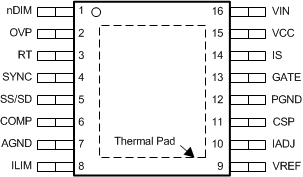
5 Pin Configuration and Functions
PWP Package
16-Pin HTSSOP With PowerPAD
Top View

Pin Functions
| PIN | TYPE | DESCRIPTION | |
|---|---|---|---|
| NAME | NO. | ||
| AGND | 7 | GND | Connect to PGND through DAP exposed thermal pad for proper ground return path. |
| COMP | 6 | I | Connect ceramic capacitor to GND to set loop compensation. |
| CSP | 11 | I | Connect to positive terminal of sense resistor in series with LED stack. |
| GATE | 13 | O | Connect to main N-channel MOSFET gate of switching converter. |
| IADJ | 10 | I | Connect resistor divider from VREF to set error amplifier reference voltage. |
| ILIM | 8 | I | Connect resistor divider from VREF to set current limit threshold voltage at IS pin. |
| IS | 14 | I | Connect to drain of main N-channel MOSFET or to source of MOSFET if sense resistor is used for improved accuracy. |
| nDIM | 1 | I | Connect resistor divider from VIN to set UVLO threshold and hysteresis. Connect through diode or MOSFET to PWM dim concurrently. |
| OVP | 2 | I | Connect resistor divider from output voltage to set OVP threshold and hysteresis. |
| PGND | 12 | GND | Connect to AGND through the exposed thermal pad for proper ground return path. |
| RT | 3 | O | Connect resistor to AGND to set base switching frequency. |
| SS/SD | 5 | I | Connect capacitor to AGND to set soft-start delay. Pull pin below 75 mV for low-power shutdown. |
| SYNC | 4 | I | Connect external PWM signal to set switching frequency. Must be higher than base frequency set at RT pin. Can also connect series resistor and capacitor to drain of main MOSFET and capacitor to AGND to implement zero-crossing detection for quasi-resonant topologies. In either case, a falling edge on SYNC triggers a new on-time at GATE. If tied to ground, internal oscillator is used. |
| VCC | 15 | O | Bypass with 2.2-µF ceramic capacitor to provide bias supply for controller. |
| VIN | 16 | I | Connect to input supply of converter. Bypass with 100-nF ceramic capacitor to AGND as close to the device as possible. |
| VREF | 9 | O | Connect to the IADJ pin directly or through resistor divider. Bypass with 100-nF ceramic capacitor to AGND. |
| Thermal Pad | GND | ||