SLVSE03B April 2019 – February 2021 TPS929120-Q1
PRODUCTION DATA
- 1 Features
- 2 Applications
- 3 Description
- 4 Revision History
- 5 Pin Configuration and Functions
- 6 Specifications
-
7 Detailed Description
- 7.1 Overview
- 7.2 Functional Block Diagram
- 7.3
Feature Description
- 7.3.1 Device Bias and Power
- 7.3.2 Constant Current Output
- 7.3.3 PWM Dimming
- 7.3.4 On-chip 8-bit Analog-to-Digital Converter (ADC)
- 7.3.5
Diagnostic and Protection in Normal State
- 7.3.5.1 Fault Masking
- 7.3.5.2 Supply Undervoltage Lockout Diagnostics in Normal State
- 7.3.5.3 Low-Supply Warning Diagnostics in Normal State
- 7.3.5.4 Reference Diagnostics in Normal State
- 7.3.5.5 Pre-Thermal Warning and Overtemperature Protection in Normal State
- 7.3.5.6 Communication Loss Diagnostic in Normal State
- 7.3.5.7 LED Open-Circuit Diagnostics in Normal State
- 7.3.5.8 LED Short-circuit Diagnostics in Normal State
- 7.3.5.9 On-Demand Off-State Invisible Diagnostics
- 7.3.5.10 On-Demand Off-State Single-LED Short-Circuit (SS) Diagnostics
- 7.3.5.11 Automatic Single-LED Short-Circuit (AutoSS) Detection in Normal State
- 7.3.5.12 EEPROM CRC Error in Normal State
- 47
- 7.3.6
Diagnostic and Protection in Fail-Safe States
- 7.3.6.1 Fault Masking
- 7.3.6.2 Supply UVLO Diagnostics in Fail-Safe States
- 7.3.6.3 Low-supply Warning Diagnostics in Fail-Safe states
- 7.3.6.4 Reference Diagnostics at Fail-Safe States
- 7.3.6.5 Overtemperature Protection in Fail-Safe State
- 7.3.6.6 LED Open-circuit Diagnostics in Fail-Safe State
- 7.3.6.7 LED Short-circuit Diagnostics in Fail-safe State
- 7.3.6.8 EEPROM CRC Error in Fail-safe State
- 57
- 7.4 Device Functional Modes
- 7.5 Programming
- 7.6 Register Maps
- 8 Application and Implementation
- 9 Power Supply Recommendations
- 10Layout
- 11Device and Documentation Support
- 12Mechanical, Packaging, and Orderable Information
Package Options
Mechanical Data (Package|Pins)
- PWP|24
Thermal pad, mechanical data (Package|Pins)
- PWP|24
Orderable Information
7.3.3.4 Exponential Brightness Control
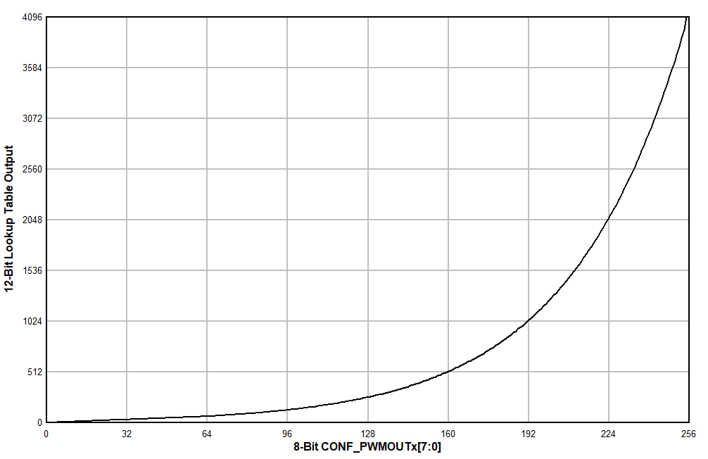
The TPS929120-Q1 can also generate PWM duty-cycle output following exponential curve. The integrated look-up table provides a one-to-one conversion from 8-bit register CONF_PWMOUTx to 12-bit binary code following exponential increment when register CONF_EXPEN is set to 1 as Figure 7-3 illustrated. When exponential control path is selected, the CONF_PWMLOWOUTx data is neglected. By using the exponential brightness control, LED brightness change by one LSB is invisible to human eyes especially at low brightness range.
 Figure 7-3 PWM Duty Cycle vs 8-bit Code for Exponential Dimming
CONF_EXPEN bit selects the dimming method between linear or exponential. Setting the bit CONF_EXPEN to 1 enables the look-up table for exponential dimming curve. In exponential PWM dimming mode, 8-bit register CONF_PWMOUTx is converted to 12-bit PWM dutycycle by look-up table automatically. Clear the bit CONF_EXPEN to 0 disables the look-up table. In this case, users must provide 12-bit PWM duty cycle. CONF_PWMOUTx stores the high 8-bit of 12-bit PWM duty-cycle information. CONF_PWMLOWOUTx stores the low 4-bit.
To avoid visible brightness flicker for exponential dimming, choose PWM frequency higher than 2 kHz through setting register CONF_PWMFREQ. Higher PWM frequency can also avoid the visible LED flash in video display due to the low beat frequency between digital camera shutter frequency and PWM frequency for LED dimming.
During power-up or in fail-safe state, the registers CONF_EXPEN, CONF_PWMOUTx, CONF_PWMFREQ are automatically reset to their default values stored in EEPROM register EEP_EXPEN, EEP_PWMOUTx, EEP_PWMFREQ. CONF_PWMLOWOUTx is reset to Fh as default value.
In fail-safe state, PWM generator only uses 8-bit EEPROM data from EEP_PWMOUTx to build PWM dutycycle output and ignores the low 4-bit. The PWM duty-cycle calculation is as shown in Equation 4.

where
- EEP_PWMOUTx is decimal number from 0 to 255.
- x is from 0 to 11 for different output channel