SLLS814A July 2007 – June 2015 TRS3221
PRODUCTION DATA.
- 1 Features
- 2 Applications
- 3 Description
- 4 Revision History
- 5 Pin Configuration and Functions
-
6 Specifications
- 6.1 Absolute Maximum Ratings
- 6.2 ESD Ratings
- 6.3 Recommended Operating Conditions
- 6.4 Thermal Information
- 6.5 Electrical Characteristics—Power
- 6.6 Electrical Characteristics—Driver
- 6.7 Electrical Characteristics—Receiver
- 6.8 Electrical Characteristics—Status
- 6.9 Switching Characteristics—Driver
- 6.10 Switching Characteristics—Receiver
- 6.11 Switching Characteristics—Status
- 6.12 Typical Characteristics
- 7 Parameter Measurement Information
- 8 Detailed Description
- 9 Application and Implementation
- 10Power Supply Recommendations
- 11Layout
- 12Device and Documentation Support
- 13Mechanical, Packaging, and Orderable Information
Package Options
Mechanical Data (Package|Pins)
- PW|16
Thermal pad, mechanical data (Package|Pins)
Orderable Information
8 Detailed Description
8.1 Overview
The TRS3221 device is a one-driver and one-receiver RS-232 interface device. All RS-232 inputs and outputs are protected up to ±15 kV using the Human-Body Model. The charge pump requires only four small 0.1-μF capacitors for operation from a 3.3-V supply. The TRS3221 device is capable of running at data rates up to 250 kbps while maintaining RS-232-compliant output levels.
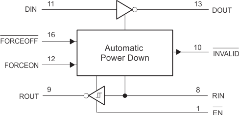
Automatic power down can be disabled when FORCEON and FORCEOFF are high. With automatic power down plus enabled, the device activates automatically when a valid signal is applied to any receiver input. The device can automatically power down the driver to save power when the RIN input is unpowered.
INVALID is high (valid data) if receiver input voltage is greater than 2.7 V or less than –2.7 V, or has been between –0.3 V and 0.3 V for less than 30 μs. INVALID is low (invalid data) if receiver input voltages are between –0.3 V and 0.3 V for more than 30 μs. Refer to Figure 7 for receiver input levels.
8.2 Functional Block Diagram

8.3 Feature Description
8.3.1 Power
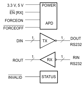
The power block increases, inverts, and regulates voltage at V+ and V– pins using a charge pump that requires four external capacitors. The automatic power-down feature for the driver is controlled by FORCEON and FORCEOFF inputs. The receiver is controlled by the EN input (see Table 1 and Table 2).
When the TRS3221 device is unpowered, it can be safely connected to an active remote RS232 device.
8.3.2 RS232 Driver
One driver interfaces standard logic level to RS232 levels. DIN input must be valid high or low.
8.3.3 RS232 Receiver
One receiver interfaces RS232 levels to standard logic levels. An open input results in a high output on ROUT. RIN input includes an internal standard RS232 load. A logic high input on the EN pin shuts down the receiver output.
8.3.4 RS232 Status
The INVALID output goes low when RIN input is unpowered for more than 30 μs. The INVALID output goes high when the receiver has a valid input. The INVALID output is active when Vcc is powered regardless of FORCEON and FORCEOFF inputs (see Table 3).
8.4 Device Functional Modes
Table 1. Driver(1)
| INPUTS | OUTPUT | DRIVER STATUS | |||
|---|---|---|---|---|---|
| DIN | FORCEON | FORCEOFF | VALID RIN RS-232 LEVEL |
DOUT | |
| X | X | L | X | Z | Powered off |
| L | H | H | X | H | Normal operation with automatic power down disabled |
| H | H | H | X | L | |
| L | L | H | Yes | H | Normal operation with automatic power down enabled |
| H | L | H | Yes | L | |
| L | L | H | No | Z | Powered off by automatic power-down feature |
| H | L | H | No | Z | |
Table 2. Receiver(1)
| INPUTS | OUTPUT | RECEIVER STATUS | ||
|---|---|---|---|---|
| RIN | EN | VALID RIN RS-232 LEVEL |
ROUT | |
| X | H | X | Z | Output off |
| L | L | X | H | Normal operation |
| H | L | X | L | |
| Open | L | No | H | |
Table 3. INVALID(1)
| INPUTS | OUTPUT | |||
|---|---|---|---|---|
| RIN | FORCEON | FORCEOFF | EN | INVALID |
| L | X | X | X | H |
| H | X | X | X | H |
| Open | X | X | X | L |
 Figure 8. Logic Diagram