SCDS343F May   2013  – August 2018 TS3DV642

PRODUCTION DATA.  

  1. Features
  2. Applications
  3. Description
    1.     Device Images
      1.      Simplified Schematic
  4. Revision History
  5. Pin Configuration and Functions
    1.     Pin Functions
  6. Specifications
    1. 6.1 Absolute Maximum Ratings
    2. 6.2 ESD Ratings
    3. 6.3 Recommended Operating Conditions
    4. 6.4 Thermal Information
    5. 6.5 Electrical Characteristics
    6. 6.6 Dynamic Characteristics
    7. 6.7 Switching Characteristics
    8. 6.8 Typical Characteristics
  7. Parameter Measurement Information
  8. Detailed Description
    1. 8.1 Overview
    2. 8.2 Functional Block Diagram
    3. 8.3 Feature Description
    4. 8.4 Device Functional Modes
  9. Application and Implementation
    1. 9.1 Application Information
    2. 9.2 Typical Application
      1. 9.2.1 Display Port (DP) Application
        1. 9.2.1.1 Design Requirements
        2. 9.2.1.2 Detailed Design Procedure
        3. 9.2.1.3 Application Curves
      2. 9.2.2 Docking Application
        1. 9.2.2.1 Design Requirements
        2. 9.2.2.2 Detailed Design Procedure
        3. 9.2.2.3 Application Curves
      3. 9.2.3 HDMI Application
        1. 9.2.3.1 Design Requirements
        2. 9.2.3.2 Detailed Design Procedure
        3. 9.2.3.3 Application Curves
  10. 10Power Supply Recommendations
  11. 11Layout
    1. 11.1 Layout Guidelines
    2. 11.2 Layout Example
  12. 12Device and Documentation Support
    1. 12.1 Receiving Notification of Documentation Updates
    2. 12.2 Community Resources
    3. 12.3 Trademarks
    4. 12.4 Electrostatic Discharge Caution
    5. 12.5 Glossary
  13. 13Mechanical, Packaging, and Orderable Information

Package Options

Mechanical Data (Package|Pins)
Thermal pad, mechanical data (Package|Pins)
Orderable Information

Typical Characteristics

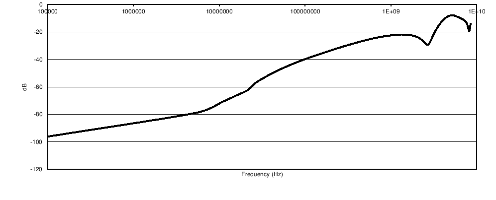
TS3DV642 tc001_cds343.gif
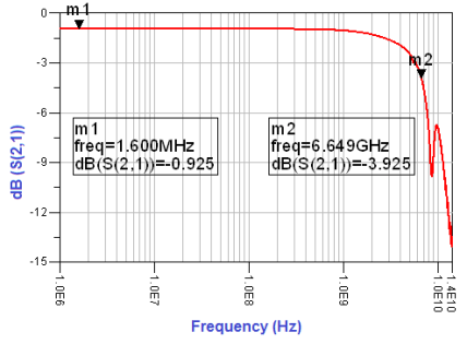
Figure 1. Differential S21 vs Frequency for Port A
TS3DV642 C001_SCDS343.png
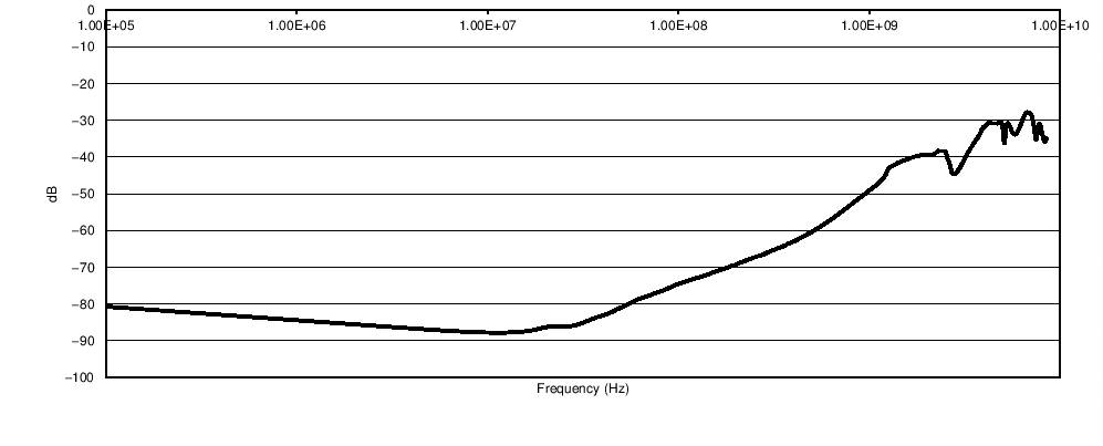
Figure 3. XTALK Port A
TS3DV642 C003_SCDS343.png
Figure 5. Off-State Isolation (OISO) for Port A
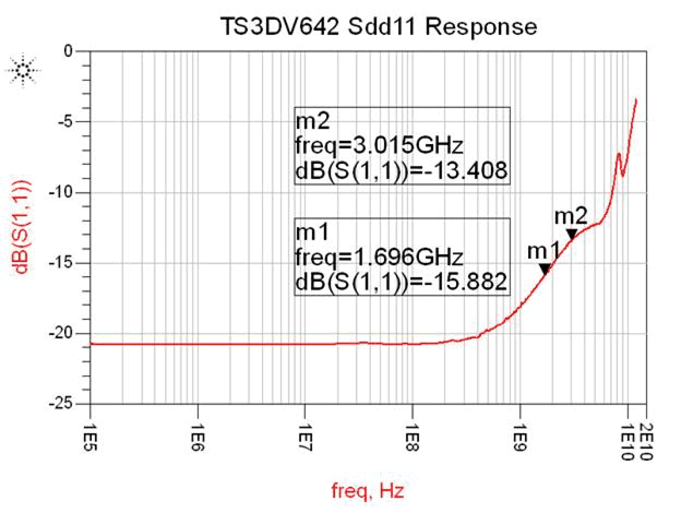
TS3DV642 SCDS343_returnloss.gifFigure 7. Return Loss (S11) Characteristics of TS3DV642
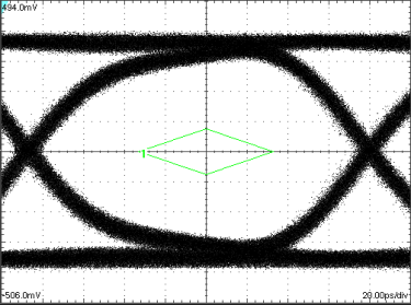
TS3DV642 tc2_scds343.gifFigure 9. Eye Pattern: 6.0 Gbps, No Device Through Path (Only One Channel Measured at a Time)
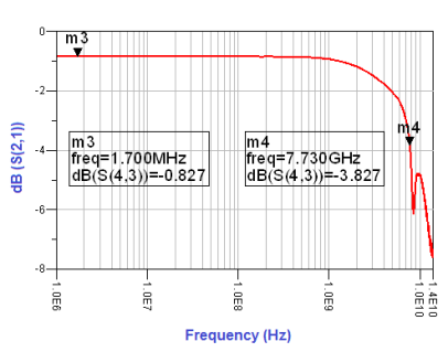
TS3DV642 tc002_cds343.gif
Figure 2. Differential S21 vs Frequency for Port B
TS3DV642 C002_SCDS343.png
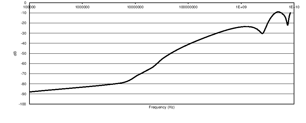
Figure 4. XTALK Port B
TS3DV642 C004_SCDS343.png
Figure 6. Off-State Isolation (OISO) for Port B
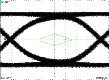
TS3DV642 tc1_scds343.gif
Figure 8. Eye Pattern: 6.0 Gbps Port A, D1+ to D1+A, D1- to D1-A (Only One Channel Measured at a Time)
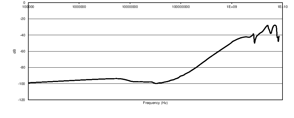
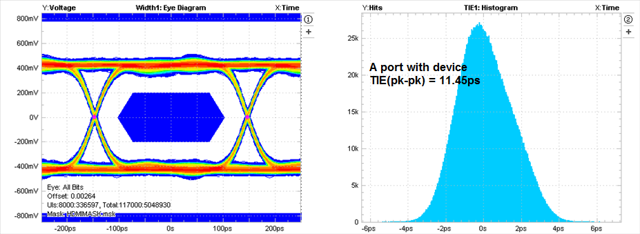
TS3DV642 A_wDevice_cds343.pngFigure 10. Eye Pattern and Time Interval Error Histogram: 3.4 Gbps Port A, With Device
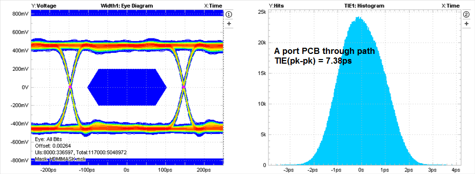
TS3DV642 A_woDevice_cds343.pngFigure 11. Eye Pattern and Time Interval Error Histogram: 3.4 Gbps, No Device Through Path
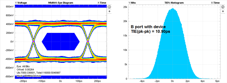
TS3DV642 B_wDevice_cds343.pngFigure 12. Eye Pattern and Time Interval Error Histogram: 3.4 Gbps Port B, With Device
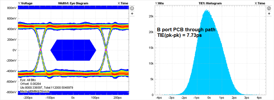
TS3DV642 B_woDevice_cds343.pngFigure 13. Eye Pattern and Time Interval Error Histogram: 3.4 Gbps Port B, No Device