SCDS328C October 2011 – August 2015 TS3USBA225
PRODUCTION DATA.
- 1 Features
- 2 Applications
- 3 Description
- 4 Revision History
- 5 Pin Configuration and Functions
- 6 Specifications
- 7 Detailed Description
- 8 Application and Implementation
- 9 Power Supply Recommendations
- 10Layout
- 11Device and Documentation Support
- 12Mechanical, Packaging, and Orderable Information
Package Options
Mechanical Data (Package|Pins)
- RUT|12
Thermal pad, mechanical data (Package|Pins)
Orderable Information
6 Specifications
6.1 Absolute Maximum Ratings(1)(2)(3)
over operating free-air temperature range (unless otherwise noted)| MIN | MAX | UNIT | |||
|---|---|---|---|---|---|
| VCC | Supply voltage | –0.3 | 6.0 | V | |
| VD0+, VD0-, VD1+, VD1- |
High speed differential signal voltage | –0.3 | 4.6 | V | |
| VR, VL | Audio signal voltage | – 1.9 | 4.6 | V | |
| IK | Analog port diode current | VI/O+ ,VI/O- < 0 | –50 | mA | |
| VI | Digital input voltage (SEL1, SEL2) | –0.3 | 6.0 | V | |
| IIK | Digital logic input clamp current(3) | VI < 0 | –50 | ||
| ICC | Continuous current through VCC | 100 | mA | ||
| IGND | Continuous current through GND | –100 | mA | ||
| Tstg | Storage temperature | –65 | 150 | °C | |
(1) Stresses beyond those listed under Absolute Maximum Ratings may cause permanent damage to the device. These are stress ratings only, and functional operation of the device at these or any other conditions beyond those indicated under Recommended Operating Conditions is not implied. Exposure to absolute-maximum-rated conditions for extended periods may affect device reliability.
(2) The algebraic convention, whereby the most negative value is a minimum and the most positive value is a maximum.
(3) All voltages are with respect to ground, unless otherwise specified.
6.2 ESD Ratings
| VALUE | UNIT | |||
|---|---|---|---|---|
| V(ESD) | Electrostatic discharge | Human-body model (HBM), per ANSI/ESDA/JEDEC JS-001(1) | ±2000 | V |
| Charged-device model (CDM), per JEDEC specification JESD22-C101(2) | ±1000 | |||
(1) JEDEC document JEP155 states that 500-V HBM allows safe manufacturing with a standard ESD control process. Manufacturing with less than 500-V HBM is possible with the necessary precautions.
(2) JEDEC document JEP157 states that 250-V CDM allows safe manufacturing with a standard ESD control process. Manufacturing with less than 250-V CDM is possible with the necessary precautions.
6.3 Recommended Operating Conditions
| MIN | MAX | UNIT | |||
|---|---|---|---|---|---|
| VCC | Supply voltage range | 2.7 | 5.0 | V | |
| VD0+, VD0-, VD1+, VD1- |
High speed differential signal voltage range | 0 | 4.5 | V | |
| VR, VL | Audio signal voltage range when not in power-down mode | –1.8 | 4.3 V or VCC(1) | V | |
| Audio signal voltage range when in power-down mode | –1 | 1 | |||
| IK | Analog port diode current | VI/O+ ,VI/O- < 0 | –50 | mA | |
| VI | Digital input voltage range (SEL1, SEL2) | 0 | VCC | V | |
| TA | Operating free-air temperature | –40 | 85 | °C | |
(1) This rating is exclusive and the voltage on the pins must not exceed either 4.3 V or VCC. E.g. if VCC = 3.3 V the voltage on the pin must not exceed 3.3 V and if VCC is = 5.0 V the voltage on the pin must not exceed 4.3 V.
6.4 Thermal Information
| THERMAL METRIC (1) | TS3USBA225 | UNIT | |
|---|---|---|---|
| RUT (UQFN) | |||
| 12 PINS | |||
| RθJA | Junction-to-ambient thermal resistance | 118.6 | °C/W |
| RθJC(top) | Junction-to-case (top) thermal resistance | 45.1 | °C/W |
| RθJB | Junction-to-board thermal resistance | 47.9 | °C/W |
| ψJT | Junction-to-top characterization parameter | 0.7 | °C/W |
| ψJB | Junction-to-board characterization parameter | 47.9 | °C/W |
(1) For more information about traditional and new thermal metrics, see the Semiconductor and IC Package Thermal Metrics application report, SPRA953.
6.5 Electrical Characteristics
TA = –40°C to 85°C, typical values are at VCC = 3.3 V, TA = 25°C (unless otherwise noted)| PARAMETER | TEST CONDITIONS | MIN | TYP | MAX | UNIT | ||
|---|---|---|---|---|---|---|---|
| MHL/USB SWITCH | |||||||
| ron | ON-state resistance | VCC = 3.0 V | VI/O+,I/O- = 0.4 V, ION = 15 mA | 6.5 | 7.5 | Ω | |
| Δron | ON-state resistance match between channels | VCC = 3.0 V | VI/O+,I/O- = 1.7 V, ION = 15 mA | 0.1 | Ω | ||
| ron (flat) | ON-state resistance flatness | VCC = 3.0 V | VI/O+,I/O- = 0 to 1.7 V, ION = 15 mA | 0.5 | Ω | ||
| IOZ | OFF leakage current | VCC = 3.6 V | Switch OFF , VI/O+,I/O- = 0 to 3.6 V, VD+/R, D-/L = 0 V |
1 | µA | ||
| USB/AUDIO SWITCH | |||||||
| ron | ON-state resistance | VCC = 3.0 V | SEL1 = High, SEL2 = Low, VL/R = –1.8 V, 0 V, 0.7 V, ION = –26 mA |
2.5 | 3.5 | Ω | |
| Δron | ON-state resistance match between channels | VCC = 3.0 V | SEL1 = High, SEL2 = Low, VL/R = 0.7 V, ION = –26 mA |
0.1 | Ω | ||
| ron (flat) | ON-state resistance flatness | VCC = 3.0 V | SEL1 = High, SEL2 = Low, VL/R = –1.8 V, 0 V, 0.7 V, ION = –26 mA |
0.1 | Ω | ||
| rSHUNT | Shunt resistance | VCC = 2.7 V to 5.0 V | Switch OFF, VL/R = 0.7 V, ISHUNT = 10 mA |
100 | 200 | Ω | |
| DIGITAL CONTROL INPUTS (SEL1, SEL2) | |||||||
| VIH | Input logic high | VCC = 3.3 V to 5.0 V | 1.3 | V | |||
| VIL | Input logic low | VCC = 2.7 V to 3.3 V | 0.25 | V | |||
| VCC = 3.3 V to 5.0 V | 0.4 | ||||||
| IIN | Input leakage current | VCC = 2.7 V to 5.0 V | VIN = 5.0 V | ±3 | μA | ||
| VIN = 0 V | ±0.1 | ||||||
| rPD1, rPD2 | Internal pulldown resistance | VCC = 2.7 V to 5.0 V | 3 | MΩ | |||
6.6 Dynamic Characteristics
TA = –40°C to 85°C, typical values are at VCC = 3.3 V, TA = 25°C (unless otherwise noted)| PARAMETER | TEST CONDITIONS | MIN | TYP | MAX | UNIT | ||
|---|---|---|---|---|---|---|---|
| MHL/USB SWITCH | |||||||
| tpd | Propagation Delay | VCC = 2.7 V or 3.3 V | 0.25 | ns | |||
| tON | Turn-on time | RL = 50 Ω, CL = 35 pF | VCC = 2.7 V | 60 | ns | ||
| tOFF | Turn-off time | RL = 50 Ω, CL = 35 pF | VCC = 2.7 V | 20 | ns | ||
| tSK(O) | Channel-to-channel skew | VCC = 2.7 V or 3.3 V | 15 | ps | |||
| tSK(P) | Skew of opposite transitions of same output | VCC = 2.7 V or 3.3 V | 15 | ps | |||
| CI/O+(OFF)
CI/O-(OFF) |
OFF capacitance | VCC = 2.7 V or 3.3 V, VD0+/D0- =0 or 3.3 V |
Switch OFF | 1 | pF | ||
| CI/O+(ON)
CI/O-(ON) |
ON capacitance | VCC = 2.7 V or 3.3 V, VD0+/D0- = 0 or 3.3 V |
Switch ON | 3 | pF | ||
| CI | Digital input capacitance | VCC = 2.7 V or 3.3 V, VI = 0 or 3.3 V | 2.5 | pF | |||
| BW | Bandwidth | VCC = 2.7 V or 3.3 V, RL = 50 Ω | Switch ON | 1.9 | GHz | ||
| OISO | OFF Isolation | VCC = 2.7 V or 3.3 V, RL = 50 Ω, f = 240 MHz |
Switch OFF | -35 | dB | ||
| XTALK | Crosstalk | VCC = 2.5 V or 3.3 V, RL = 50 Ω, f = 240 MHz |
Switch ON | -45 | dB | ||
| USB/AUDIO SWITCH | |||||||
| tON | Turn-on time | RL = 50 Ω, CL = 35 pF | VCC = 2.7 V | 40 | µs | ||
| tOFF | Turn-off time | RL = 50 Ω, CL = 35 pF | VCC = 2.7 V | 15 | ns | ||
| CL(OFF), CR(OFF) | L , R OFF capacitance | VCC = 2.7 V to 4.5 V, f = 20 kHz | Switch OFF | 1.0 | pF | ||
| CL(ON), CR(ON) | L, R ON capacitance | VCC = 2.7 V to 4.5 V, f = 20 kHz | Switch ON | 3.5 | pF | ||
| OISO | OFF Isolation | VCC = 3.3 V, RL = 50 Ω, f = 20 kHz | Switch OFF | -85 | dB | ||
| XTALK | Crosstalk | VCC = 3.3 V, RL = 50 Ω, f = 20 kHz | Switch ON | -95 | dB | ||
| THD | Total harmonic distortion | VCC = 3.3 V, SEL1 = High, SEL2 = Low, f = 20 Hz to 20 kHz, RL = 600 Ω, VIN = 2 Vpp |
Switch ON | 0.05% | |||
| SUPPLY | |||||||
| VCC | Power supply voltage | 2.7 | 5.0 | V | |||
| ICC | Positive supply current | VCC = 2.7 V, 3.6 V, 5.0 V VIN= VCC or GND, VI/O = 0 V, Switch ON or OFF |
25 | 50 | µA | ||
| ICC, PD | Positive supply current (Power-Down Mode) | VCC = 2.7 V, 3.6 V, 5.0 V, VI/O = 0 V, SEL1 and SEL2 = Low |
3 | 5 | µA | ||
| PSRR | Power Supply Rejection Ratio | VCC = 2.7 V, 3.6 V, 5.0 V VIN = VCC +/- 200 mVpp RL = 50 Ω |
-60 | dB | |||
| IOFF | Power off leakage current | VCC = 0 V, D+/R, D-/L, D0+, D0-, D1+, D1-, L, VIN = 0 to 4.5 V |
±0.1 | µA | |||
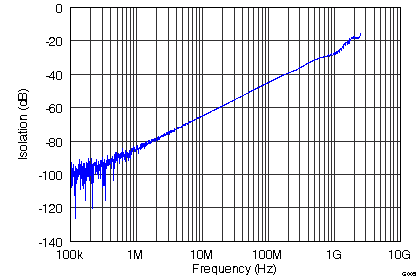
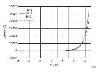
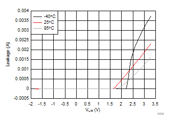
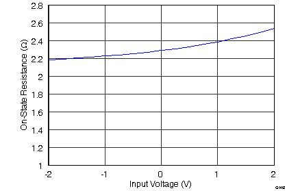
6.7 Typical Characteristics
A.
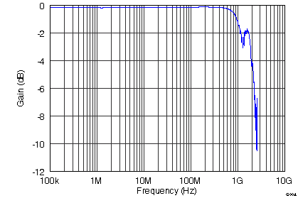
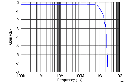
Figure 3. Gain vs Frequency for MHL/USB Switch
