SCDS336C November 2012 – October 2016 TS5A3159-Q1
PRODUCTION DATA.
- 1 Features
- 2 Applications
- 3 Description
- 4 Revision History
- 5 Pin Configuration and Functions
-
6 Specifications
- 6.1 Absolute Maximum Ratings
- 6.2 ESD Ratings
- 6.3 Recommended Operating Conditions
- 6.4 Thermal Information
- 6.5 Electrical Characteristics for 5-V Supply
- 6.6 Electrical Characteristics for 3.3-V Supply
- 6.7 Electrical Characteristics For 2.5-V Supply
- 6.8 Electrical Characteristics For 1.8-V Supply
- 6.9 Typical Characteristics
- 7 Parameter Measurement Information
- 8 Detailed Description
- 9 Applications and Implementation
- 10Power Supply Recommendations
- 11Layout
- 12Device and Documentation Support
- 13Mechanical, Packaging, and Orderable Information
Package Options
Refer to the PDF data sheet for device specific package drawings
Mechanical Data (Package|Pins)
- DBV|6
Thermal pad, mechanical data (Package|Pins)
Orderable Information
7 Parameter Measurement Information
Table 1. Parameter Description
| SYMBOL | DESCRIPTION |
|---|---|
| VCOM | Voltage at COM |
| VNC | Voltage at NC |
| VNO | Voltage at NO |
| ron | Resistance between COM and NC or COM and NO ports, when the channel is ON |
| rpeak | Peak ON-state resistance over a specified voltage range |
| ∆ron | Difference of ron between channels |
| ron(flat) | Difference between the maximum and minimum value of ron in a channel over the specified range of conditions |
| INC(OFF) | Leakage current measured at the NC port, with the corresponding channel (NC to COM) in the OFF state under worst-case input and output conditions |
| INO(OFF) | Leakage current measured at the NO port, with the corresponding channel (NO to COM) in the OFF state under worst-case input and output conditions |
| INC(ON) | Leakage current measured at the NC port, with the corresponding channel (NC to COM) in the ON state and the output (COM) being open |
| INO(ON) | Leakage current measured at the NO port, with the corresponding channel (NO to COM) in the ON state and the output (COM) being open |
| ICOM(ON) | Leakage current measured at the COM port, with the corresponding channel (COM to NO or COM to NC) in the ON state and the output (NC or NO) being open |
| VIH | Minimum input voltage for logic high for the control input (IN) |
| VIL | Minimum input voltage for logic low for the control input (IN) |
| VIN | Voltage at IN |
| IIH, IIL | Leakage current measured at IN |
| tON | Turn-on time for the switch. This parameter is measured under the specified range of conditions and by the propagation delay between the digital control (IN) signal and analog outputs (COM, NC, or NO) signal, when the switch is turning ON. |
| tOFF | Turn-off time for the switch. This parameter is measured under the specified range of conditions and by the propagation delay between the digital control (IN) signal and analog outputs (COM, NC, or NO) signal, when the switch is turning OFF. |
| tBBM | Break-before-make time. This parameter is measured under the specified range of conditions and by the propagation delay between the output of two adjacent analog channels (NC and NO), when the control signal changes state. |
| QC | Charge injection is a measurement of unwanted signal coupling from the control (IN) input to the analog (NC, NO, or COM) output. This is measured in coulomb (C) and measured by the total charge induced due to switching of the control input. Charge injection, QC = CL × ∆VO, CL is the load capacitance, and ∆VO is the change in analog output voltage. |
| CNC(OFF) | Capacitance at the NC port when the corresponding channel (NC to COM) is OFF |
| CNO(OFF) | Capacitance at the NO port when the corresponding channel (NO to COM) is OFF |
| CNC(ON) | Capacitance at the NC port when the corresponding channel (NC to COM) is ON |
| CNO(ON) | Capacitance at the NO port when the corresponding channel (NO to COM) is ON |
| CCOM(ON) | Capacitance at the COM port when the corresponding channel (COM to NC or COM to NO) is ON |
| CIN | Capacitance of IN |
| OISO | OFF isolation of the switch is a measurement OFF-state switch impedance. This is measured in dB in a specific frequency, with the corresponding channel (NC to COM or NO to COM) in the OFF state. |
| XTALK | Crosstalk is a measurement of unwanted signal coupling from an ON channel to an OFF channel (NC to NO or NO to NC). This is measured in a specific frequency and in dB. |
| BW | Bandwidth of the switch. This is the frequency in which the gain of an ON channel is −3 dB below the DC gain. |
| I+ | Static power-supply current with the control (IN) pin at V+ or GND |
| ∆I+ | This is the increase in I+ for each control (IN) input that is at the specified voltage, rather than at V+ or GND. |
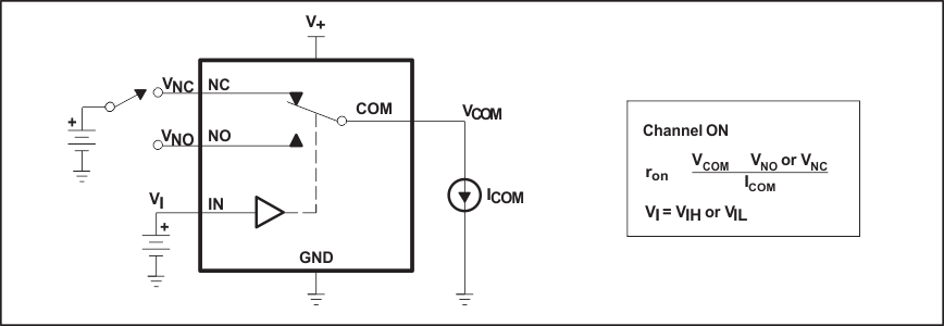 Figure 9. On-State Resistance (ron)
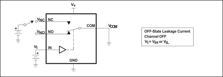 Figure 10. Off-State Leakage Current (INC(OFF), INO(OFF))
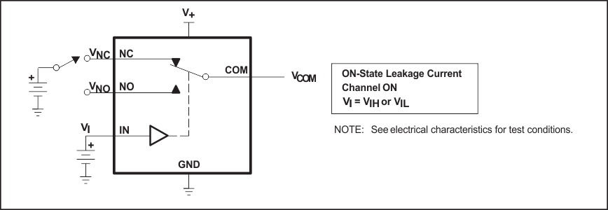 Figure 11. On-State Leakage Current (ICOM(ON), INC(ON), INO(ON))
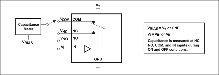 Figure 12. Capacitance (CI, CCOM(ON), CNC(OFF), CNO(OFF), CNC(ON), CNO(ON))
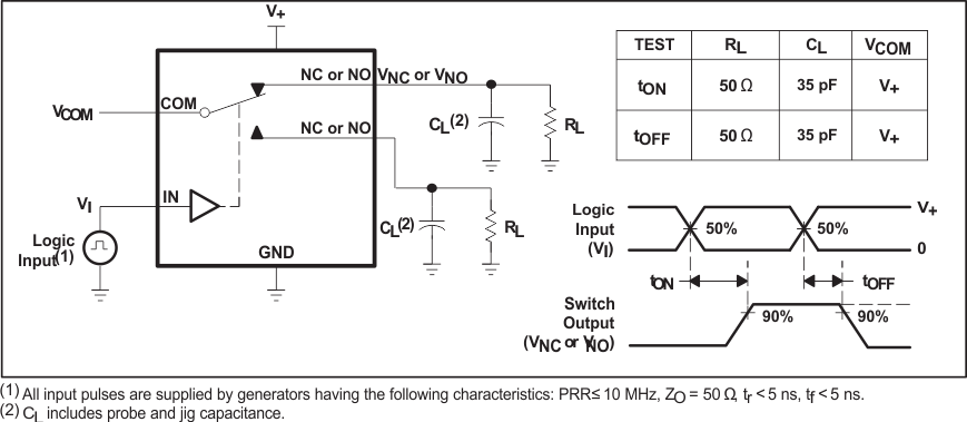 Figure 13. Turn-On (tON) and Turn-Off Time (tOFF)
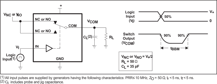 Figure 14. Break-Before-Make Time (tBBM)
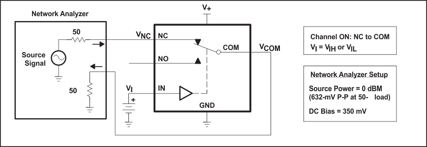 Figure 15. Bandwidth (BW)
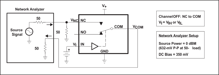 Figure 16. OFF Isolation (OISO)
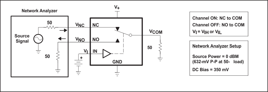 Figure 17. Crosstalk (XTALK)
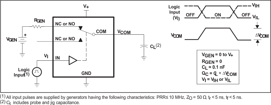 Figure 18. Charge Injection (QC)
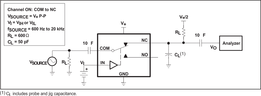 Figure 19. Total Harmonic Distortion (THD)