SCDS335A September 2012 – August 2014 TSU8111
PRODUCTION DATA.
- 1 Features
- 2 Applications
- 3 Description
- 4 Revision History
- 5 Pin Configuration and Functions
- 6 Specifications
-
7 Detailed Description
- 7.1 Overview
- 7.2 Functional Block Diagram
- 7.3 Feature Description
- 7.4 Device Functional Modes
- 7.5 Programming
- 7.6
Register Map
- 7.6.1 Device ID (01h) Register Field Descriptions
- 7.6.2 Control (02h) Register Field Descriptions
- 7.6.3 Interrupt 1 (03h) Register Field Descriptions
- 7.6.4 Interrupt 2 (04h) Register Field Descriptions
- 7.6.5 Interrupt Mask 1 (05h) Register Field Descriptions
- 7.6.6 Interrupt Mask 2 (06h) Register Field Descriptions
- 7.6.7 ADC (07h) Register Field Descriptions
- 7.6.8 Timing Set 1 (08h) Register Field Descriptions
- 7.6.9 Timing Set 2 (09h) Register Field Descriptions
- 7.6.10 Device Type 1 (0Ah) Register Field Descriptions
- 7.6.11 Device Type 2 (0Bh) Register Field Descriptions
- 7.6.12 Button 1 (0Ch) Register Field Descriptions
- 7.6.13 Button 2 (0Dh) Register Field Descriptions
- 7.6.14 Manual SW 1 (13h) Register Field Descriptions
- 7.6.15 Manual SW 2 (14h) Register Field Descriptions
- 7.6.16 Reset (1Bh) Register Field Descriptions
- 7.6.17 Charger control 1 (20h) Register Field Descriptions
- 7.6.18 Charger control 2 (21h) Register Field Descriptions
- 7.6.19 Battery Charger Control 3 (22h) Register Field Descriptions
- 7.6.20 Charger Interrupt (24h) Register Field Descriptions
- 7.6.21 Charger Interrupt Mask (25h) Register Field Descriptions
- 7.6.22 Charger Status (26h) Register Field Descriptions
- 8 Application and Implementation
- 9 Power Supply Recommendations
- 10Layout
- 11Device and Documentation Support
- 12Mechanical, Packaging, and Orderable Information
Package Options
Mechanical Data (Package|Pins)
- YFP|20
Thermal pad, mechanical data (Package|Pins)
Orderable Information
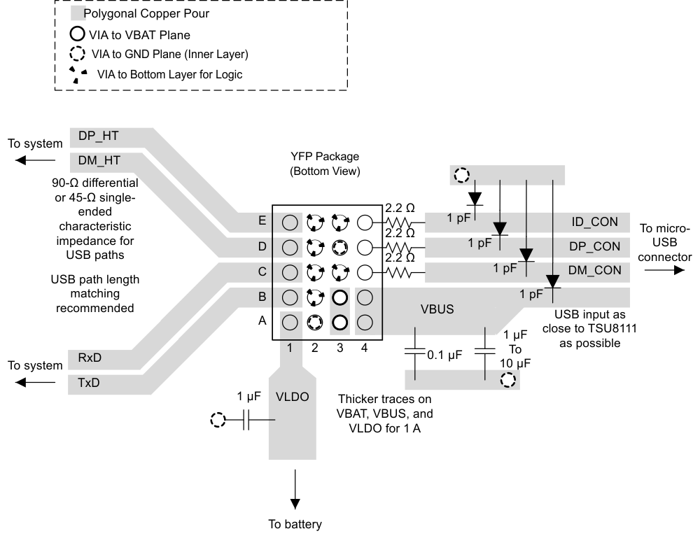
10 Layout
10.1 Layout Guidelines
- The TSU8111 should be placed as close to the USB connector as possible to reduce the effect of stray noise.
- Decoupling capacitors, as mentioned in Power Supply Recommendations, should be as close to the device as possible. This will also reduce the effect of ESR and ripple seen on voltages due to transient spikes.
- Lengths of all traces should be kept less than 2 inches.
- For 1-oz copper thickness, the width of the USB traces should be at least 15 mils.
- Traces to the VBAT, VBUS, and VLDO pins should be capable of carrying 1 A. This will keep routing resistance less than 100-mΩ and minimize voltage drops when charging with high currents.
- Maximize the use of vias on VBUS, VBAT, and GND. Increasing the number of vias will reduce routing resistance and improve thermal performance.
- Minimize the use of vias for USB traces to preserve USB signal integrity.
- All USB traces (DP_CON, DM_CON, DP_HT, DM_HT, TxD, and RxD) should have 45-Ω single-ended impedance and 90-Ω differential impedance to fulfill USB 2.0 requirements.
10.2 Layout Example