SLLSEF7 March 2014 TUSB8020B-Q1
PRODUCTION DATA.
- 1 Features
- 2 Applications
- 3 Description
- 4 Revision History
- 5 Description (Continued)
- 6 Terminal Configuration and Functions
- 7 Specifications
-
8 Detailed Description
- 8.1 Overview
- 8.2 Functional Block Diagram
- 8.3 Feature Description
- 8.4 Device Functional Modes
- 8.5
Register Maps
- 8.5.1
Configuration Registers
- 8.5.1.1 ROM Signature Register
- 8.5.1.2 Vendor ID LSB Register
- 8.5.1.3 Vendor ID MSB Register
- 8.5.1.4 Product ID LSB Register
- 8.5.1.5 Product ID MSB Register
- 8.5.1.6 Device Configuration Register
- 8.5.1.7 Battery Charging Support Register
- 8.5.1.8 Device Removable Configuration Register
- 8.5.1.9 Port Used Configuration Register
- 8.5.1.10 PHY Custom Configuration Register
- 8.5.1.11 Device Configuration Register 2
- 8.5.1.12 UUID Registers
- 8.5.1.13 Language ID LSB Register
- 8.5.1.14 Language ID MSB Register
- 8.5.1.15 Serial Number String Length Register
- 8.5.1.16 Manufacturer String Length Register
- 8.5.1.17 Product String Length Register
- 8.5.1.18 Serial Number Registers
- 8.5.1.19 Manufacturer String Registers
- 8.5.1.20 Product String Registers
- 8.5.1.21 Additional Feature Configuration Register
- 8.5.1.22 Charging Port Control Register
- 8.5.1.23 Device Status and Command Register
- 8.5.1
Configuration Registers
- 9 Applications and Implementation
- 10Power Supply Recommendations
- 11Layout
- 12Device and Documentation Support
- 13Mechanical, Packaging, and Orderable Information
Package Options
Mechanical Data (Package|Pins)
- PHP|48
Thermal pad, mechanical data (Package|Pins)
- PHP|48
Orderable Information
11 Layout
11.1 Layout Guidelines
11.1.1 Placement
- 9.53K ±1% resistor connected to terminal USB_R1 should be placed as close as possible to the TUSB8020B-Q1.
- A 0.1-µF capacitor should be placed as close as possible on each VDD and VDD33 power pin.
- The 100-nF capacitors on the SSTXP and SSTXM nets should be placed close to the USB connector (Type A, Type B, and so forth).
- The ESD and EMI protection devices (if used) should also be placed as possible to the USB connector.
- If a crystal is used, it must be placed as close as possible to the TUSB8020B-Q1’s XI and XO terminals.
- Place voltage regulators as far away as possible from the TUSB8020B-Q1, the crystal, and the differential pairs.
- In general, the large bulk capacitors associated with each power rail should be placed as close as possible to the voltage regulators.
11.1.2 Package Specific
- The TUSB8020B-Q1 package as a 0.5-mm pin pitch.
- The TUSB8020B-Q1 package has a 3.6-mm x 3.6-mm thermal pad. This thermal pad must be connected to ground through a system of vias.
- All vias under device, except for those connected to thermal pad, should be solder masked to avoid any potential issues with thermal pad layouts.
11.1.3 Differential Pairs
This section describes the layout recommendations for all the TUSB8020B-Q1 differential pairs: USB_DP_XX, USB_DM_XX, USB_SSTXP_XX, USB_SSTXM_XX, USB_SSRXP_XX, and USB_SSRXM_XX.
- Must be designed with a differential impedance of 90 Ω ±10%.
- In order to minimize cross talk, it is recommended to keep high speed signals away from each other. Each pair should be separated by at least 5 times the signal trace width. Separating with ground as depicted in the layout example will also help minimize cross talk.
- Route all differential pairs on the same layer adjacent to a solid ground plane.
- Do not route differential pairs over any plane split.
- Adding test points will cause impedance discontinuity and will therefore negative impact signal performance. If test points are used, they should be placed in series and symmetrically. They must not be placed in a manner that causes stub on the differential pair.
- Avoid 90° turns in trace. The use of bends in differential traces should be kept to a minimum. When bends are used, the number of left and right bends should be as equal as possible and the angle of the bend should be ≥ 135°. This will minimize any length mismatch causes by the bends and therefore minimize the impact bends have on EMI.
- Minimize the trace lengths of the differential pair traces. The maximum recommended trace length for SS differential pair signals and USB 2.0 differential pair signals is eight inches. Longer trace lengths require very careful routing to assure proper signal integrity.
- Match the etch lengths of the differential pair traces (i.e. DP and DM or SSRXP and SSRXM or SSTXP and SSTXM). There should be less than 5 mils difference between a SS differential pair signal and its complement. The USB 2.0 differential pairs should not exceed 50 mils relative trace length difference.
- The etch lengths of the differential pair groups do not need to match (i.e. the length of the SSRX pair to that of the SSTX pair), but all trace lengths should be minimized.
- Minimize the use of vias in the differential pair paths as much as possible. If this is not practical, make sure that the same via type and placement are used for both signals in a pair. Any vias used should be placed as close as possible to the TUSB8020B-Q1 device.
- To ease routing, the polarity of the SS differential pairs can be swapped. This means that SSTXP can be routed to SSTXM or SSRXM can be routed to SSRXP.
- Do not place power fuses across the differential pair traces.
11.2 Layout Example
11.2.1 Upstream Port
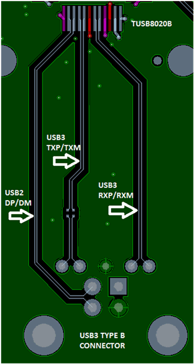 Figure 14. Example Routing of Upstream Port
11.2.2 Downstream Port
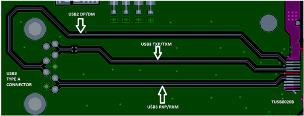 Figure 15. Example Routing of Downstream Port
11.2.3 Thermal Pad
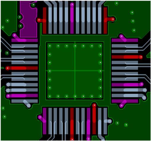 Figure 16. Example Thermal Pad Layout