SLVSED5C december 2017 – august 2023 TVS2200
PRODUCTION DATA
- 1
- 1 Features
- 2 Applications
- 3 Description
- 4 Revision History
- 5 Device Comparison Table
- 6 Pin Configuration and Functions
- 7 Specifications
- 8 Detailed Description
- 9 Application and Implementation
- 10Device and Documentation Support
- 11Mechanical, Packaging, and Orderable Information
Package Options
Mechanical Data (Package|Pins)
- DRV|6
Thermal pad, mechanical data (Package|Pins)
- DRV|6
Orderable Information
3 Description
The TVS2200 robustly shunts up to 40 A of IEC 61000-4-5 fault current to protect systems from high power transients or lightning strikes. The device offers a solution to the common industrial signal line EMC requirement to survive up to ±1 kV IEC 61000-4-5 open circuit voltage coupled through a 42 Ω impedance.
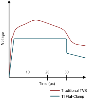
The TVS2200 uses a unique feedback mechanism for precise flat clamping during a fault, allowing system exposure below 30 V. The tight voltage regulation allows designers to confidently select system components with a lower voltage tolerance, lowering system costs and complexity without sacrificing robustness.
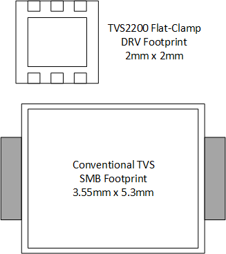
In addition, the TVS2200 is available in a small 2 mm × 2 mm SON footprint which is designed for space constrained applications, offering a 70 percent reduction in size compared to industry standard SMA and SMB packages. The extremely low device leakage and capacitance causes a minimal effect on the protected line. For robust protection over the lifetime of the product, TI tests the TVS2200 against 5,000 repetitive surge strikes at high temperature with no shift in device performance.
The TVS2200 is part of TI's Flat-Clamp family of surge devices. For more information on the other devices in the family, see the Device Comparison Table.
 Footprint Comparison
 Voltage Clamp Response to 8
µs to 20 µs Surge Event