SCES854A May 2014 – September 2017 TXS0102-Q1
PRODUCTION DATA.
- 1 Features
- 2 Applications
- 3 Description
- 4 Revision History
- 5 Pin Configuration and Functions
-
6 Specifications
- 6.1 Absolute Maximum Ratings
- 6.2 ESD Ratings
- 6.3 Recommended Operating Conditions
- 6.4 Thermal Information
- 6.5 Electrical Characteristics
- 6.6 Timing Requirements — VCCA = 1.8 V ± 0.15 V
- 6.7 Timing Requirements — VCCA = 2.5 V ± 0.2 V
- 6.8 Timing Requirements — VCCA = 3.3 V ± 0.3 V
- 6.9 Switching Characteristics — VCCA = 1.8 V ± 0.15 V
- 6.10 Switching Characteristics — VCCA = 2.5 V ± 0.2 V
- 6.11 Switching Characteristics — VCCA = 3.3 V ± 0.3 V
- 6.12 Typical Characteristics
- 7 Parameter Measurement Information
- 8 Detailed Description
- 9 Application and Implementation
- 10Power Supply Recommendations
- 11Layout
- 12Device and Documentation Support
- 13Mechanical, Packaging, and Orderable Information
Package Options
Mechanical Data (Package|Pins)
- DCU|8
Thermal pad, mechanical data (Package|Pins)
Orderable Information
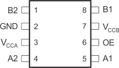
5 Pin Configuration and Functions
DCU Package
8-Pin VSSOP
Top View

Pin Functions
| PIN | I/O | DESCRIPTION | |
|---|---|---|---|
| NAME | NO. | ||
| A1 | 5 | I/O | Input-output 1 for the A port. This pin is referenced to VCCA. |
| A2 | 4 | I/O | Input-output 2 for the A port. This pin is referenced to VCCA. |
| B1 | 8 | I/O | Input-output 1 for the B port. This pin is referenced to VCCB. |
| B2 | 1 | I/O | Input-output 2 for the B port. This pin is referenced to VCCB. |
| GND | 2 | — | Ground |
| OE | 6 | I | Tri-state output-mode enable. Pull the OE pin low to place all outputs in tri-state mode. This pin is referenced to VCCA. |
| VCCA | 3 | — | A-port supply voltage. 1.65 V ≤ VCCA ≤ 3.6 V and VCCA ≤ VCCB. |
| VCCB | 7 | — | B-port supply voltage. 2.3 V ≤ VCCB ≤ 5.5 V. |