SGLS318A November 2005 – November 2015 UC2854B-EP
PRODUCTION DATA.
- 1 Features
- 2 Applications
- 3 Description
- 4 Revision History
- 5 Description (continued)
- 6 Pin Configuration and Functions
- 7 Specifications
- 8 Detailed Description
-
9 Application and Implementation
- 9.1 Application Information
- 9.2
Typical Application
- 9.2.1 Design Requirements
- 9.2.2
Detailed Design Procedure
- 9.2.2.1 Switching Frequency
- 9.2.2.2 Inductor Selection
- 9.2.2.3 Output Capacitor
- 9.2.2.4 Switch and Diode
- 9.2.2.5 Current Sensing
- 9.2.2.6 Peak Current Limit
- 9.2.2.7 Multiplier Set-up
- 9.2.2.8 Feedforward Voltage
- 9.2.2.9 Multiplier Input Current
- 9.2.2.10 Oscillator Frequency
- 9.2.2.11 Current Error Amplifier Compensation
- 9.2.2.12 Voltage Error Amplifier Compensation
- 9.2.2.13 Feedforward Voltage Divider Filter Capacitors
- 9.2.2.14 Design Procedure Summary
- 9.2.3 Application Curve
- 10Power Supply Recommendations
- 11Layout
- 12Device and Documentation Support
- 13Mechanical, Packaging, and Orderable Information
Package Options
Mechanical Data (Package|Pins)
- DW|16
Thermal pad, mechanical data (Package|Pins)
- DW|16
Orderable Information
11 Layout
11.1 Layout Guidelines
As in any converter design, Layout is a critical portion of good power supply design.
Always try to use a low EMI inductor with a ferrite type closed core. Some examples would be toroid and encased E core inductors. Open core can be used if they have low EMI characteristics and are located a bit more away from the low power traces and components. Make the poles perpendicular to the PCB as well if using an open core. Stick cores usually emit the most unwanted noise.
Several signals paths that conduct fast changing currents or voltages can interact with stray inductance or parasitic capacitance to generate noise or degrade the power supplies performance.
• To help eliminate these problems, the Vcc pin should be bypassed to ground with a low ESR ceramic bypass capacitor with X5R or X7R dielectric.
• Care should be taken to minimize the loop area formed by the bypass capacitor connections, the Vcc pins, and the ground connections.
Try to run the feedback trace as far from the inductor and noisy power traces as possible. You would also like the feedback trace to be as direct as possible and somewhat thick. These two sometimes involve a trade-off, but keeping it away from inductor EMI and other noise sources is the more critical of the two. Run the feedback trace on the side of the PCB opposite of the inductor with a ground plane separating the two.
External compensation components for stability should also be placed close to the IC. Surface mount components are recommended here as well for the same reasons discussed for the filter capacitors. These should not be located very close to the inductor either.
Control circuitry and its associated components should be laid out minimizing the stray inductive loops.
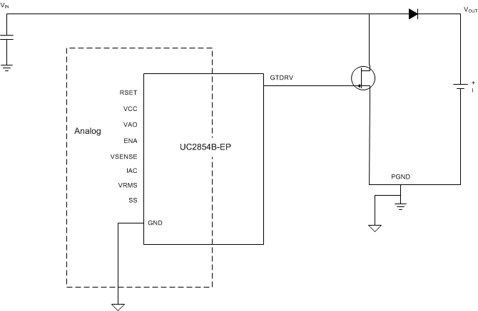
11.2 Layout Example
 Figure 13. Layout Recommendation