SLUSCK0F November 2017 – February 2024 UCC21220 , UCC21220A
PRODUCTION DATA
- 1
- 1 Features
- 2 Applications
- 3 Description
- 4 Device Comparison Table
- 5 Pin Configuration and Functions
-
6 Specifications
- 6.1 Absolute Maximum Ratings
- 6.2 ESD Ratings
- 6.3 Recommended Operating Conditions
- 6.4 Thermal Information
- 6.5 Power Ratings
- 6.6 Insulation Specifications
- 6.7 Safety-Related Certifications
- 6.8 Safety-Limiting Values
- 6.9 Electrical Characteristics
- 6.10 Switching Characteristics
- 6.11 Thermal Derating Curves
- 6.12 Typical Characteristics
- 7 Parameter Measurement Information
- 8 Detailed Description
-
9 Application and Implementation
- 9.1 Application Information
- 9.2
Typical Application
- 9.2.1 Design Requirements
- 9.2.2
Detailed Design Procedure
- 9.2.2.1 Designing INA/INB Input Filter
- 9.2.2.2 Select External Bootstrap Diode and its Series Resistor
- 9.2.2.3 Gate Driver Output Resistor
- 9.2.2.4 Estimating Gate Driver Power Loss
- 9.2.2.5 Estimating Junction Temperature
- 9.2.2.6 Selecting VCCI, VDDA/B Capacitor
- 9.2.2.7 Application Circuits with Output Stage Negative Bias
- 9.2.3 Application Curves
- 10Power Supply Recommendations
- 11Layout
- 12Device and Documentation Support
- 13Revision History
- 14Mechanical, Packaging, and Orderable Information
Package Options
Mechanical Data (Package|Pins)
- D|16
Thermal pad, mechanical data (Package|Pins)
Orderable Information
3 Description
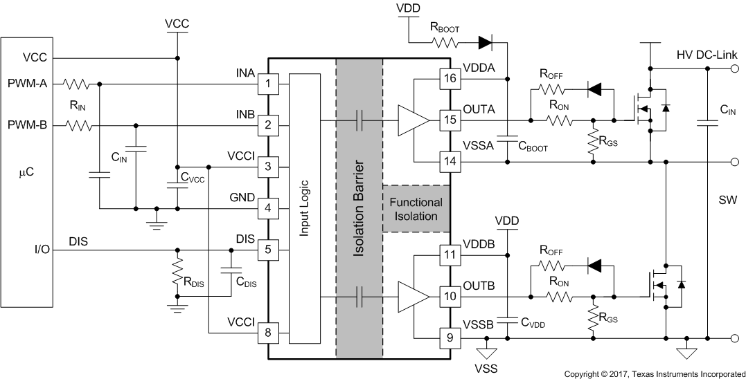
The UCC21220 and UCC21220A devices are basic and functional isolated dual-channel gate drivers with 4A peak-source and 6A peak-sink current. They are designed to drive power MOSFETs and GaNFETs in PFC, Isolated DC/DC, and synchronous rectification applications, with fast switching performance and robust ground bounce protection through greater than 100V/ns common-mode transient immunity (CMTI).
These devices can be configured as two low-side drivers, two high-side drivers, or half-bridge drivers. Two outputs can be paralleled to form a single driver which doubles the drive strength for heavy load conditions due to the best-in-class delay matching performance.
Protection features include the following: DIS pin shuts down both outputs simultaneously when it is set high, INA/B pin rejects input transient shorter than 5ns, both inputs and outputs can withstand –2V spikes for 200ns, all supplies have undervoltage lockout (UVLO), and active pulldown protection clamps the output below 2.1V when unpowered or floated.
With these features, these devices enable high efficiency, high power density, and robustness in a wide variety of power applications.
 Typical Application