SLUSDC0C October 2018 – November 2021 UCC21530
PRODUCTION DATA
- 1 Features
- 2 Applications
- 3 Description
- 4 Revision History
- 5 Pin Configuration and Functions
-
6 Specifications
- 6.1 Absolute Maximum Ratings
- 6.2 ESD Ratings
- 6.3 Recommended Operating Conditions
- 6.4 Thermal Information
- 6.5 Power Ratings
- 6.6 Insulation Specifications
- 6.7 Safety-Related Certifications
- 6.8 Safety-Limiting Values
- 6.9 Electrical Characteristics
- 6.10 Switching Characteristics
- 6.11 Insulation Characteristics Curves
- 6.12 Typical Characteristics
- 7 Parameter Measurement Information
- 8 Detailed Description
-
9 Application and Implementation
- 9.1 Application Information
- 9.2
Typical Application
- 9.2.1 Design Requirements
- 9.2.2 Detailed Design Procedure
- 9.2.3 Application Curves
- 10Power Supply Recommendations
- 11Layout
- 12Device and Documentation Support
Package Options
Mechanical Data (Package|Pins)
- DWK|14
Thermal pad, mechanical data (Package|Pins)
Orderable Information
9.2 Typical Application
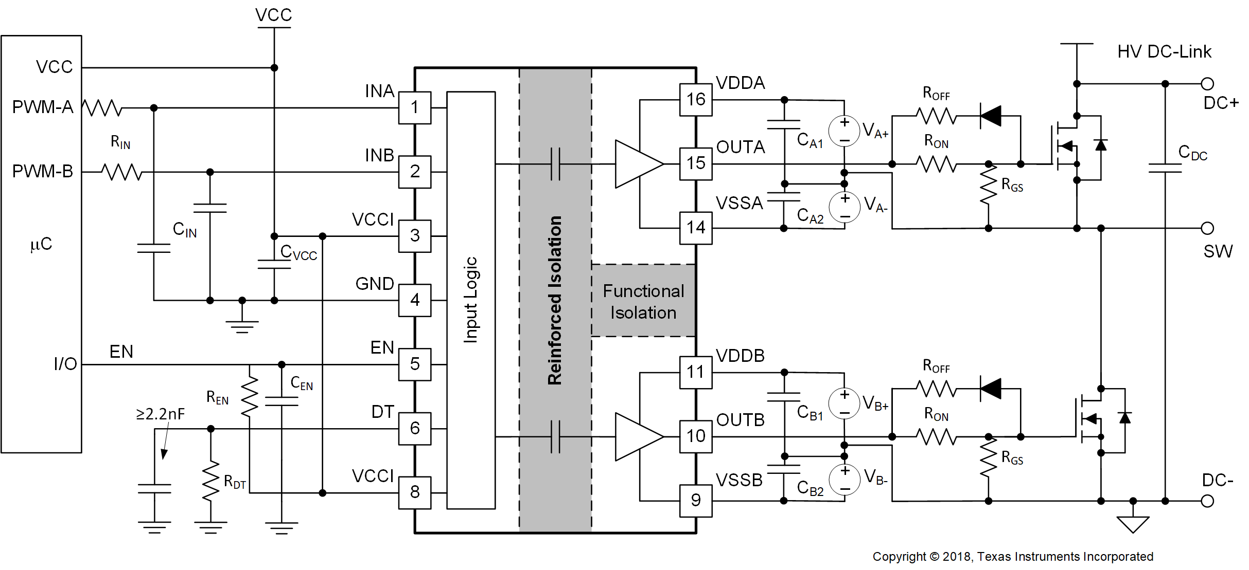
The circuit in Figure 9-1 shows a reference design with UCC21530 driving a typical half-bridge configuration which could be used in several popular power converter topologies such as synchronous buck, synchronous boost, half-bridge/full bridge isolated topologies, and 3-phase motor drive applications. This circuit uses two supplies (or single-input-double-output power supply). Power supply VA+ determines the positive drive output voltage and VA– determines the negative turn-off voltage. The configuration for channel B is the same as channel A.
When parasitic inductances are introduced by non-ideal PCB layout and long package leads (e.g. TO-220 and TO-247 type packages), there could be ringing in the gate-source drive voltage of the power transistor during high di/dt and dv/dt switching. If the ringing is over the threshold voltage, there is the risk of unintended turn-on and even shoot-through. Applying a negative bias on the gate drive is a popular way to keep such ringing below the threshold. This solution has two separate power supplies for each driver channel, so it provides flexibility when setting the positive and negative rail voltages.
 Figure 9-1 Typical Application Schematic with Dual Power Supplies