SLUSBL6 February 2015 UCC24650
PRODUCTION DATA.
- 1 Features
- 2 Applications
- 3 Description
- 4 Revision History
- 5 Pin Configuration and Functions
- 6 Specifications
- 7 Detailed Description
- 8 Application and Implementation
- 9 Power Supply Recommendations
- 10Layout
- 11Device and Documentation Support
- 12Mechanical, Packaging, and Orderable Information
Package Options
Mechanical Data (Package|Pins)
- DBV|5
Thermal pad, mechanical data (Package|Pins)
Orderable Information
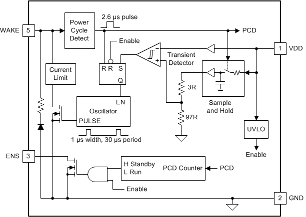
7 Detailed Description
7.1 Overview
The UCC24650 is a voltage monitor designed to alert a companion primary-side controller device when the monitor detects a relative droop of approximately 3% on its VDD input. Commonly known as a wake-up device, the UCC24650 is normally used in isolated-flyback power supply applications using primary-side regulation (PSR). Because the PSR controller may operate at very-low frequencies during light-load or no-load conditions, it cannot detect a sudden load step that may occur between power cycles and the output voltage may fall out of regulation. The UCC24650 can detect the voltage droop and wake-up a compatible PSR controller to increase its switching frequency before the output falls too low. This action significantly reduces the amount of output capacitance needed to achieve an acceptable transient response.
At the end of each power cycle delivered by the PSR controller, the UCC24650 droop monitor refreshes an internally stored voltage scaled to 97% of the VDD voltage. If the monitor detects a droop of VDD to the level of the stored voltage, the WAKE signal is connected to GND by an internal low-impedance switch. The WAKE signal transmits a current pulse across the isolation transformer to a compatible PSR controller, such as the UCC28730, capable of detecting the wake-up signal on the primary side of the transformer.
The UCC24650 is also capable of disabling a compatible SR controller, such as the UCC24610, during light-load conditions to minimize standby power. The ENS output signal is driven low after a fixed sustained count of low-frequency power pulses, and can re-enable the SR controller after a cumulative count of 32 higher-frequency power pulses. The ENS output may also be used to drive other secondary circuitry compatible with the ENS operating parameters.
7.2 Functional Block Diagram
7.3 Feature Description
7.3.1 UVLO Block
The UCC24650 device can operate over a bias supply voltage range from approximately 4 to 28 V. All functions are disabled and bias supply current is quiescent until the UVLO turn-on threshold is exceeded. When enabled, all functions remain operational until the VDD voltage falls below the UVLO turn-off threshold.
To ensure that wake-up pulses can be successfully driven, make sure the output voltage droop at VDD during a load-step does not fall below the maximum UVLO turn-off threshold before at least one wake-up pulse can be issued. This imposes a practical limit on the lowest nominal no-load voltage allowable at VDD before the maximum load step is applied.
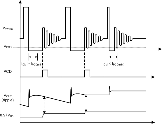
7.3.2 PCD
After the UCC24650 has been turned on and enabled, the WAKE pin is used to detect the power-cycle waveforms at the flyback transformer secondary winding. This winding voltage can be at wide-ranging levels, but the PCD block arms the sample-and-hold (S&H) block to acquire a reference voltage reading at VDD when certain criteria are met. The PCD block triggers the S&H block at the end of the demagnetization time, tDM, provided that the voltage at WAKE has remained below the VPCD threshold for longer than tPCD(min), to ensure that the sampled voltage is free of transient deviations and noise. Consequently, this imposes a minimum demagnetization-time constraint on the flyback design to provide adequate signal for the PCD function.
Figure 11 illustrates the behavior of the device for power-cycles that do meet the criteria and for those that do not. The wake-up reference voltage, which is stored internally as approximately 97% of the sampled VDD voltage, is updated at every PCD pulse to change proportionally with the changes in output voltage. Disturbances at the WAKE input which do not meet the PCD criteria do not affect the stored reference voltage.
7.3.3 Sample, Hold, and Transient Detector
The sample-and-hold function (S&H) monitors the VDD voltage, samples that voltage during a PCD pulse, and holds the buffered sample constant during the interval between power cycles. The held sample is scaled to about 97% of the external voltage to serve as a –3% droop-detection threshold reference voltage. The external VDD voltage is continually compared to the internal droop reference by the transient detection comparator, and a wake-up signal is triggered if VDD falls below the droop-reference voltage.
The S&H droop-reference voltage is refreshed at the end of each power cycle detected by the PCD function, to track minor changes in output voltage. The droop-reference voltage is held accurately for PCD intervals less than tSW(max), but may drift either higher or lower during longer intervals.
7.3.4 Wake Pulse Generator and WAKE Switch
The WAKE pin not only functions as a PCD input as described in PCD, but also serves as an output driver to accomplish the wake-up function. An integrated N-channel MOSFET switch is connected between WAKE and GND and is driven by the WAKE-pulse oscillator when the conditions for wake-up are met (see Functional Block Diagram). Each wake-up pulse is of short duration to limit internal dissipation and is repeated periodically until a PSR-driven power cycle is detected or until VDD has fallen to the UVLO turn-off threshold.
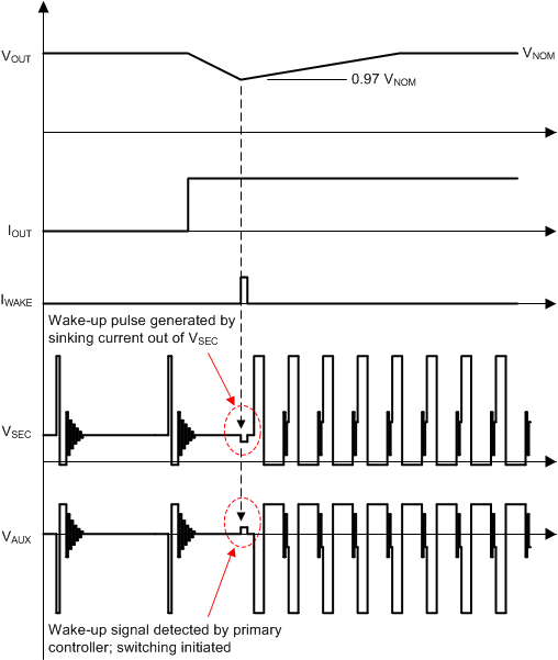
Figure 13 shows two possible typical system responses. The solid lines indicate the successful wake-up of a compatible PSR controller from the sleeping or Wait state between low-frequency power cycles. After a load step causes the output voltage (at VDD) to cross the previously stored reference voltage, the WAKE output drives a current pulse to the PSR controller which responds with multiple power cycles to restore regulation. At each power cycle, the reference voltage is refreshed and further WAKE pulses are suppressed. In the case where the PSR controller does not respond to the first wake-up pulse, the dotted lines indicate that the wake-up pulses are repeated, the reference voltage is not refreshed, and the output voltage continues to fall.
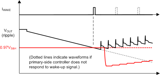 Figure 13. System Response to Wake-Up Signal After Load-Transient Event
In the event that a power cycle occurs during the droop before VOUT has reached the WAKE threshold, the S&H reference is updated to the VOUT voltage at that moment. This may extend the droop by another 3% before the WAKE threshold is reached and the condition for a wake-up signal is met, effectively delaying the wake-up as illustrated by Figure 14 and Figure 15.
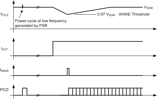 Figure 14. Simplified Typical System Response to Wake-Up Signal After Load-Transient Event
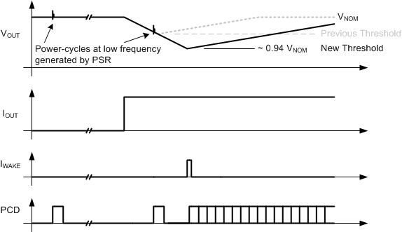 Figure 15. Simplified Delayed System Response to Wake-Up Signal After Load-Transient Event
The typical on-state resistance of the WAKE switch is approximately 150 Ω at 25°C and varies with junction temperature. Consequently, the wake-pulse current capability in low-voltage applications also varies with temperature (see Figure 7 in the Typical Characteristics). A built-in current limit prevents excess pulse current and power dissipation in higher-voltage applications.
In a typical isolated-flyback PSR topology, the wake-pulse current establishes a signal voltage across the system impedance, which consists mainly of the parallel combination of the primary magnetizing inductance, LM, and the switched-node capacitance, CSWN, scaled by the transformer turns-ratio.
In applications with higher output voltages, some rectifier diodes may exhibit high forward voltage drop characteristics, along with possible additional voltage due to package inductance and stray inductance. This negative forward voltage is impressed on the WAKE input with respect to GND, as shown in Figure 16.
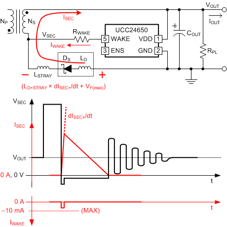 Figure 16. High dISEC/dt may Generate Significant IWAKE.
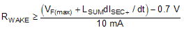
To avoid exceeding the maximum source-current rating for WAKE (see Absolute Maximum Ratings), a series resistance may be required to limit the WAKE current. Its value is calculated by Equation 1. However, this resistance presents additional impedance to the WAKE signal current that can be developed. Do not oversize RWAKE to avoid depressing the Wake-Up signal level at the PSR detection input. A trade-off between the level of reverse-current limiting and the WAKE signal drive level may be necessary.
where
- VF(max) is the highest forward voltage drop expected.
- LSUM is the combined stray and package inductance.
7.3.5 PCD Counter and ENS Switch
Some PSR applications may use an SR in place of the output diode rectifier to improve efficiency. For applications using the UCC24610 SR controller, the UCC24650 device provides the ENS output which can be used to enable the SR controller when the switching frequency is high, and disable it when the switching frequency is very low, to reduce standby power dissipation. Although the ENS function is specifically optimized for use with the UCC24610 device, it may also be used for other purposes provided the ENS pin is operated within its specified limits.
The ENS output consists of an open-drain, N-channel MOSFET switch with on-resistance of approximately 2.7 kΩ at 25°C. A PCD counter (see Functional Block Diagram) monitors the time intervals between pulses and determines whether to turn on or off the ENS switch. At power-up, the ENS switch is off (high-impedance open-drain state) by default, and remains that way as long as the power-cycle period, tSW, is less than the disable qualifying interval, tDISS, to keep the SR controller enabled. After tSW > tDISS for a count of at least 63 consecutive power cycles, the ENS switch is turned on (low-impedance to GND) to disable the SR controller. This disable-count is reset to zero if any switching cycle period occurs where tSW < tDISS. This consecutive count requirement ensures that the switching frequency is consistently low enough to justify disabling the SR controller to minimize its bias power.
There is considerable hysteresis in the qualifying interval timing, so the ENS switch remains on (SR or other secondary circuit is disabled) until tSW becomes less than the enable qualifying interval, tENS. In other words, the switching frequency is increasing. When tSW < tENS for 32 cumulative power cycles, the ENS switch is turned off and the SR controller is enabled. When ENS is in the Low state, the cumulative count allows any number of switching cycles with tSW > tENS without resetting the count. Figure 17 and Figure 18 show these ENS state transitions based on the switching period timing and interval count.
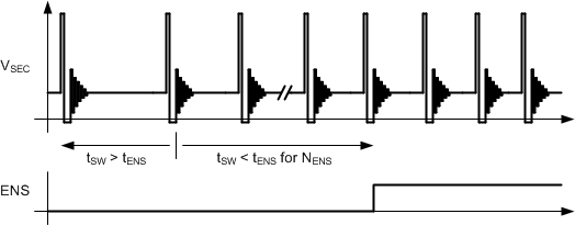
Only 32 shorter tSW intervals are necessary to re-enable the SR controller to avoid excess rectifier dissipation as the system load increases. However, these shorter intervals (higher frequency) are not required to be consecutive, so that ENS is allowed to toggle High eventually, even if the switching frequency is not yet consistently higher. This method ensures that the SR or other circuitry is not prevented from re-enabling if the frequency is not consistent due to variable loads.
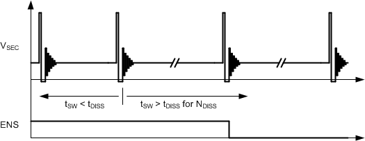
At least 63 consecutive counts of tSW > tDISS are necessary to disable the SR controller, to ensure that random deviations in tSW do not unnecessarily disrupt normal SR operation. In this manner, the ENS function is heavily skewed in favor of keeping the SR controller enabled, unless it is consistently operated at a very-low frequency, particularly during no-load operation. ENS is not affected in the case of a wake-up event, and the count is not changed. After a wake-up, the switching frequency generally increases quite rapidly, so the ENS switch is turned off to re-enable the SR controller as soon as the count of tSW < tENS reaches 32. Depending on the previous cumulative switching period history, the time to re-enable the SR controller may be anywhere between 32 switching cycles and immediate.
7.4 Device Functional Modes
The UCC24650 operates as a voltage monitor in either of two modes: ENS output is High (driver is off), or ENS output is Low (driver is on). In either mode, when the monitor detects a 3% droop in the VDD voltage, it triggers a Wake-Up signal on the WAKE pin.