SLUSD60 October 2017 UCC256304
PRODUCTION DATA.
- 1 Features
- 2 Applications
- 3 Description
- 4 Revision History
- 5 Pin Configuration and Functions
- 6 Specifications
-
7 Detailed Description
- 7.1 Overview
- 7.2 Functional Block Diagram
- 7.3
Feature Description
- 7.3.1 Hybrid Hysteretic Control
- 7.3.2 Regulated 12-V Supply
- 7.3.3 Feedback Chain
- 7.3.4 Optocoupler Feedback Signal Input and Bias
- 7.3.5 System External Shut Down
- 7.3.6 Pick Lower Block and Soft Start Multiplexer
- 7.3.7 Pick Higher Block and Burst Mode Multiplexer
- 7.3.8 VCR Comparators
- 7.3.9 Resonant Capacitor Voltage Sensing
- 7.3.10 Resonant Current Sensing
- 7.3.11 Bulk Voltage Sensing
- 7.3.12 Output Voltage Sensing
- 7.3.13 High Voltage Gate Driver
- 7.3.14 Protections
- 7.4 Device Functional Modes
-
8 Application and Implementation
- 8.1 Application Information
- 8.2
Typical Application
- 8.2.1 Design Requirements
- 8.2.2
Detailed Design Procedure
- 8.2.2.1 Custom Design With WEBENCH® Tools
- 8.2.2.2 LLC Power Stage Requirements
- 8.2.2.3 LLC Gain Range
- 8.2.2.4 Select Ln and Qe
- 8.2.2.5 Determine Equivalent Load Resistance
- 8.2.2.6 Determine Component Parameters for LLC Resonant Circuit
- 8.2.2.7 LLC Primary-Side Currents
- 8.2.2.8 LLC Secondary-Side Currents
- 8.2.2.9 LLC Transformer
- 8.2.2.10 LLC Resonant Inductor
- 8.2.2.11 LLC Resonant Capacitor
- 8.2.2.12 LLC Primary-Side MOSFETs
- 8.2.2.13 Design Considerations for Adaptive Dead-Time
- 8.2.2.14 LLC Rectifier Diodes
- 8.2.2.15 LLC Output Capacitors
- 8.2.2.16 HV Pin Series Resistors
- 8.2.2.17 BLK Pin Voltage Divider
- 8.2.2.18 BW Pin Voltage Divider
- 8.2.2.19 ISNS Pin Differentiator
- 8.2.2.20 VCR Pin Capacitor Divider
- 8.2.2.21 Burst Mode Programming
- 8.2.2.22 Soft-Start Capacitor
- 8.2.3 Application Curves
- 9 Power Supply Recommendations
- 10Layout
- 11Device and Documentation Support
- 12Mechanical, Packaging, and Orderable Information
Package Options
Mechanical Data (Package|Pins)
- DDB|14
Thermal pad, mechanical data (Package|Pins)
Orderable Information
8 Application and Implementation
NOTE
Information in the following applications sections is not part of the TI component specification, and TI does not warrant its accuracy or completeness. TI’s customers are responsible for determining suitability of components for their purposes. Customers should validate and test their design implementation to confirm system functionality.
8.1 Application Information
UCC256304 can be used in a wide range of applications in which LLC topology is implemented. In order to make the part easier to use, TI has prepared a list of materials to demonstrate the features of the device:
- Full featured EVM hardware
- A excel design calculator
- Simulation models
- Application notes on Hybrid Hysteretic Control theory
In the following sections, a typical design example is presented.
8.2 Typical Application
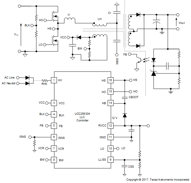
Shown below is a typical half bridge LLC application using UCC256304 as the controller.
8.2.1 Design Requirements
The design specifications are summarized in Table 8.
Table 8. System Design Specifications
| PARAMETER | TEST CONDITIONS | MIN | TYP | MAX | UNITS | |
|---|---|---|---|---|---|---|
| INPUT CHARACTERISTICS | ||||||
| DC Voltage range | 340 | 390 | 410 | VDC | ||
| AC Voltage range | 85 | 264 | VAC | |||
| AC Voltage frequency | 47 | 63 | Hz | |||
| Input DC UVLO On | 120 | VDC | ||||
| Input DC UVLO Off | 102 | VDC | ||||
| Input DC current | Input = 340 VDC, full load = 10 A | 0.383 | A | |||
| Input DC current | Input = 390 VDC, full load = 10 A | 0.331 | A | |||
| Input DC current | Input = 410 VDC, full load = 10 A | 0.315 | A | |||
| OUTPUT CHARACTERISTICS | ||||||
| Output voltage, VOUT | No load to full load | 12 | VDC | |||
| Output load current, IOUT | 340 VDC to 410 VDC | 10 | A | |||
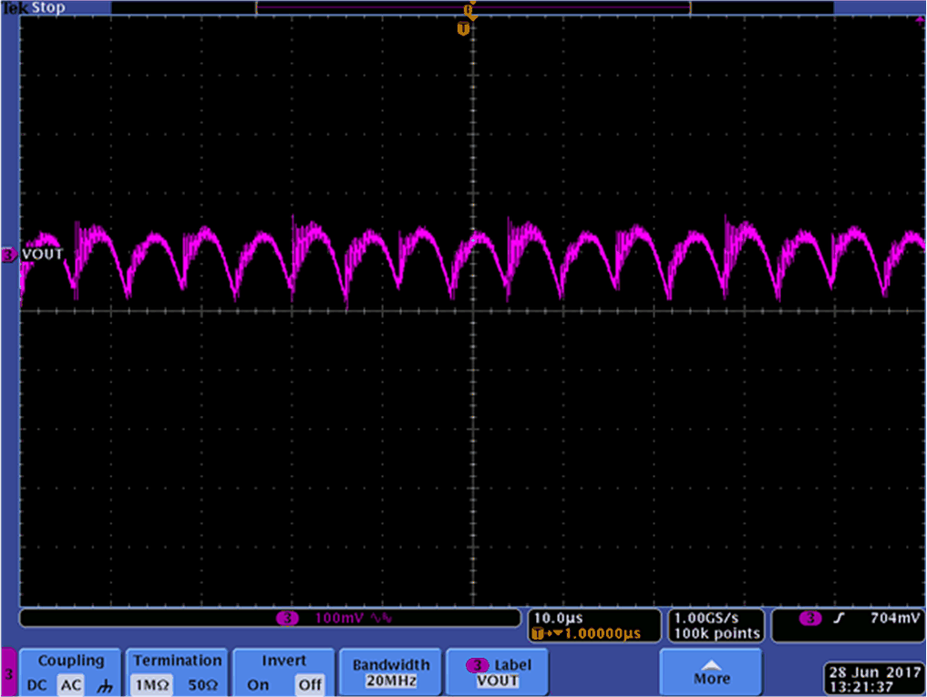
| Output voltage ripple | 390 VDC and full load = 10 A | 130 | mVpp | |||
| SYSTEMS CHARACTERISTICS | ||||||
| Switching frequency | 53 | 160 | kHz | |||
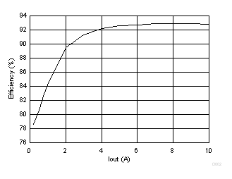
| Peak efficiency | 390 VDC | 92.9 | ||||
| Operating temperature | Natural convection | 25 | ºC | |||
8.2.2 Detailed Design Procedure
8.2.2.1 Custom Design With WEBENCH® Tools
Click here to create a custom design using the UCC256304 device with the WEBENCH® Power Designer.
- Start by entering the input voltage (VIN), output voltage (VOUT), and output current (IOUT) requirements.
- Optimize the design for key parameters such as efficiency, footprint, and cost using the optimizer dial.
- Compare the generated design with other possible solutions from Texas Instruments.
The WEBENCH Power Designer provides a customized schematic along with a list of materials with real-time pricing and component availability.
In most cases, these actions are available:
- Run electrical simulations to see important waveforms and circuit performance
- Run thermal simulations to understand board thermal performance
- Export customized schematic and layout into popular CAD formats
- Print PDF reports for the design, and share the design with colleagues
Get more information about WEBENCH tools at www.ti.com/WEBENCH.
8.2.2.2 LLC Power Stage Requirements
Start the design by deciding the LLC power stage component values. The LLC power stage design procedure outlined here follows the one given in the TI application note “Designing an LLC Resonant Half-Bridge Power Converters”. The application note contains a full explanation of the origin of each of the equations used. The equations given below are based on the First Harmonic Approximation (FHA) method commonly used to analyze the LLC topology. This method gives a good starting point for any design, but a final design requires an iterative approach combining the FHA results, circuit simulation, and hardware testing. An alternative design approach is given in TI application note SLUA733, LLC Design for UCC29950.
8.2.2.3 LLC Gain Range
First, determine the transformer turns ratio by the nominal input and output voltages.

Then determine the LLC gain range Mg(min) and Mg(max). Assume there is a 0.5-V drop in the rectifier diodes (Vf) and a further 0.5-V drop due to other losses (Vloss).


8.2.2.4 Select Ln and Qe
Ln is the ratio between the magnetizing inductance and the resonant inductance.

Qe is the quality factor of the resonant tank.

In this equation, Re is the equivalent load resistance.
Selecting Ln and Qe values should result in an LLC gain curve, as shown below, that intersects with Mg(min) and Mg(max) traces. The peak gain of the resulting curve should be larger than Mg(max). Details of how to select Ln and Qe are not discussed here. They are available in the Application Note, UCC25630x Practical Design Guidelines and UCC256304 Design Calculator.
In this case, the selected Ln and Qe values are:


8.2.2.5 Determine Equivalent Load Resistance
Determine the equivalent load resistance by Equation 17.

8.2.2.6 Determine Component Parameters for LLC Resonant Circuit
Before determining the resonant tank component parameters, a nominal switching frequency (resonant frequency) should be selected. In this design, 100 kHz is selected as the resonant frequency.

The resonant tank parameters can be calculated as the following:


After the preliminary parameters are selected, find the closest actual component value that is available, re-check the gain curve with the selected parameters, and then run time domain simulation to verify the circuit operation.
The following resonant tank parameters are:


Based on the final resonant tank parameters, the resonant frequency can be calculated:

Based on the new LLC gain curve, the normalized switching frequency at maximum and minimum gain are given by:


The maximum and minimum switching frequencies are:


8.2.2.7 LLC Primary-Side Currents
The primary-side currents are calculated for component selection purpose. The currents are calculated based on a 110% overload condition.
The primary side RMS load current is given by:

The RMS magnetizing current at minimum switching frequency is given by:

The total current in resonant tank is given by:

8.2.2.8 LLC Secondary-Side Currents
The total secondary side RMS load current is the current referred from the primary side current (Ioe) to the secondary side.

In this design, the transformer’s secondary side has a center-tapped configuration. The current of each secondary transformer winding is calculated by:

The corresponding half-wave average current is:

8.2.2.9 LLC Transformer
A bias winding is needed in order to utilize the HV self start up function. It is recommended to design the bias winding so that the VCC voltage is greater than 13 V.
The transformer can be built or purchased according to these specifications:
- Turns ratio: Primary : Secondary : Bias = 32 : 2 : 3
- Primary terminal voltage: 450Vac
- Primary magnetizing inductance: LM = 830 µH
- Primary side winding rated current: Ir = 1.009 A
- Secondary terminal voltage: 36Vac
- Secondary winding rated current: Iws = 8.639 A
- Minimum switching frequency: 50.3 kHz
- Maximum switching frequency: 111.3 kHz
- Insulation between primary and secondary sides: IEC60950 reinforced insulation
The minimum operating frequency during normal operation is that calculated above but during shutdown the LLC can operate at right above ZCS boundary condition, which is a lower frequency. The magnetic components in the resonant circuit, the transformer and resonant inductor, should be rated to operate at this lower frequency.
8.2.2.10 LLC Resonant Inductor
The AC voltage across the resonant inductor is given by its impedance times the current:

The inductor can be built or purchased according to the following specifications:
- Inductance: Lr = 61.5 µH
- Rated current: Ir = 1.009 A
- Terminal AC voltage:
- Frequency range: 50.3 kHz to 111.3 kHz
The minimum operating frequency during normal operation is that calculated above but during shutdown the LLC can operate at right above ZCS boundary condition, which is a lower frequency. The magnetic components in the resonant circuit, the transformer and resonant inductor, should be rated to operate at this lower frequency.
8.2.2.11 LLC Resonant Capacitor
This capacitor carries the full-primary current at a high frequency. A low dissipation factor part is needed to prevent overheating in the part.
The AC voltage across the resonant capacitor is given by its impedance times the current.


Peak voltage:

Valley voltage:

Rated current:

8.2.2.12 LLC Primary-Side MOSFETs
Each MOSFET sees the input voltage as its maximum applied voltage. Choose the MOSFET voltage rating to be 1.5 times of the maximum bulk voltage:

Choose the MOSFET current rating to be 1.1 times of the maximum primary side RMS current:

8.2.2.13 Design Considerations for Adaptive Dead-Time
After the resonant tank is designed and the primary side MOSFET is selected, the ZVS operation of the converter needs to be double checked. ZVS can only be achieved when there is enough current left in the resonant inductor at the gate turn off edge to discharge the switch node. UCC256304 implements adaptive dead-time based on the slewing of the switch node. The slew detection circuit has a detection range of 1V/ns to 50 V/ns.
To check the ZVS operation, a series of time domain simulations are conducted, and the resonant current at the gate turn off edges are captured. An example plot is shown below:
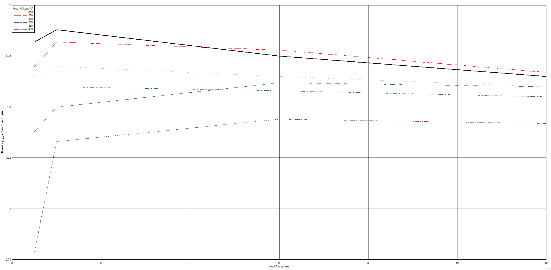 Figure 54. Adaptive Dead-Time
The figure above assumes the maximum switching frequency occurs at 5% load, and system starts to burst at 5% load.
From this plot, the minimum resonant current left in the tank is Imin = 0.8 A in the interested operation range. In order to calculate the slew rate, the primary side switch node parasitic capacitance must be known. This value can be estimated from the MOSFET datasheet. In this case, Cswitchnode = 400 pF. The minimum slew rate is given by:

This is larger than 1 V/ns minimum detectable slew rate.
8.2.2.14 LLC Rectifier Diodes
The voltage rating of the output diodes is given by:

The current rating of the output diodes is given by:

8.2.2.15 LLC Output Capacitors
The LLC converter topology does not require an output filter although a small second stage filter inductor may be useful in reducing peak-to-peak output noise. Assuming that the output capacitors carry the rectifier’s full wave output current then the capacitor ripple current rating is:

Use 20 V rating for 12-V output voltage:

The capacitor’s RMS current rating is:

Solid Aluminum capacitors with conductive polymer technology have high ripple-current ratings and are a good choice here. The ripple-current rating for a single capacitor may not be sufficient so multiple capacitors are often connected in parallel.
The ripple voltage at the output of the LLC stage is a function of the amount of AC current that flows in the capacitors. To estimate this voltage, assume that all the current, including the DC current in the load, flows in the filter capacitors.

The capacitor specifications are:
- Voltage Rating: 20 V
- Ripple Current Rating: 4.84 A
- ESR: < 19 mΩ
8.2.2.16 HV Pin Series Resistors
Multiple resistors are connected in series with HV pin to limit the power dissipation of the UCC256304 device. The recommended series resistor with HV pin is 5 kΩ.
8.2.2.17 BLK Pin Voltage Divider
BLK pin senses the LLC input voltage and determines when to turn on and off the LLC converter. Different versions of UCC256304 have different BLK thresholds.
Choose bulk startup voltage at 340 V, then the BLK resistor divider ratio can be calculated as below:

The desired power consumption of the BLK pin resistor divider is PBLKsns = 10 mW. The BLK sense resistor total value is given by:

The lower BLK divider resistor value is given by:

The higher BLK divider resistor value is given by:

The actual bulk voltage thresholds can be calculated:


8.2.2.18 BW Pin Voltage Divider
BW pin senses the output voltage through the bias winding and protects the power stage from over voltage. The nominal output voltage is 12 V. The bias winding has 3 turns, and the secondary side winding has 2 turns. So the nominal voltage of the bias winding is given by:

The desired OVP threshold in this design is 115% of the nominal value. The OVP threshold level in UCC256304 device is 4 V, so the nominal BW pin voltage is given by:

Choose the lower resistor of the BW resistor divider to be 10 kΩ.

The upper resistor can be calculated by:

8.2.2.19 ISNS Pin Differentiator
ISNS pin sets the over current protection level. OCP1 is peak current protection level; OCP2 and OCP3 are average current protection levels. The threshold voltages are 0.6 V, 0.8 V, and 4 V, respectively.
Set OCP3 level at 150% of full load. Thus, the sensed average input current level at full load is given by:

The current sense ratio can then be calculated:

Select a current sense capacitor first, since there are less high voltage capacitor choices than resistors:

Then calculate the required ISNS resistor value:

After the current sense ratio is determined, the peak ISNS pin voltage at full load can be calculated:

The peak resonant current at OCP1 level is given by:

The peak secondary-side current at OCP1 level is given by:

8.2.2.20 VCR Pin Capacitor Divider
The capacitor divider on the VCR pin sets two parameters: (1) the divider ratio of the resonant capacitor voltage; (2) the amount of frequency compensation to be added. The first criteria the capacitor divider needs to meet is that under over load condition, the peak-to-peak voltage on VCR pin is with in 6 V.
As derived earlier, the following relationship between VCOMP voltage, ΔVCR, switching period, input average current, and the VCR capacitor divider is shown in Equation 70

In this equation, C1 is the upper capacitor on the capacitor divider; C2 is the lower capacitor on the capacitor divider. VCOMP is contributed by two parts – the divided resonant capacitor voltage, and the voltage generated by the VCR pin internal current sources. Define the contribution of the internal current source to be KVCRRamp.

Select C1 and C2 so that KVCRRamp is within 0.1 ~ 0.6 range, and at over load condition, VCOMP is less than 6 V. In this example C1 = 150 pF and C2 = 15 nF is select.
8.2.2.21 Burst Mode Programming
The burst mode programming interface enables user to program a burst mode threshold voltage (VLL) which adaptively changes with input voltage. This way, consistent burst threshold can be achieved across VIN range, thus making the efficiency curve more consistent across VIN range.
The following relationship exists between VLL voltage and BLK pin voltage:

In this equation, VLL is the burst mode threshold voltage; VBLK is BLK pin voltage; two parameters a and b can be programmed by two external resistors.
After soft start is done, the sensed BLK pin voltage is applied to LL/SS pin from inside the IC through a buffer. As shown in the figure below, this creates a difference between the current flowing through the programming resistor RLLUpper and RLLLower. The difference between the current flows into the LL/SS pin, mirrored and then applied to a 250-kΩ resistor RLL. The voltage on RLL is used as VLL.
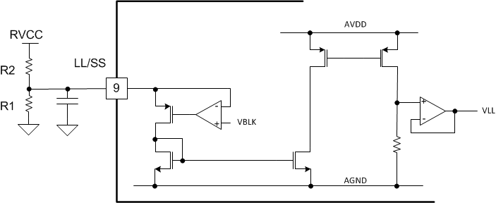 Figure 55. Burst Mode Programming
The relationship between VLL and VBLK can then be derived:

Equation 73 rearranged produces Equation 74

To determine RLLUpper and RLLLower, two sets of (VLL, VBLK) values are required. VBLK can be measured directly from BLK pin. VLL level can be measured by inserting a 10-kΩ resistor between the feedback optocoupler emitter and ground. Assume the voltage measured on the 10-kΩ resistor is V10k. Then VLL voltage can be calculated as:

Remove the RLLUpper. In this way, the VLL voltage is at its minimal value 0.7 V, which is determined by the internal circuit design. Then adjust the load current to the desired burst mode threshold load level, and make sure the power stage does not burst in this condition. For example, 10% load is the desired burst mode threshold level. With 10 A as the full-load condition, set the load current to 1 A. After the load current is set, change the input voltage to two different voltages and record two different readings (V10k, VBLK). Then based on Equation 74 and Equation 75, RLLUpper and RLLLower can be solved.
In this example select the lower resistor to be 402 kΩ and the upper resistor to be 732 kΩ.
8.2.2.22 Soft-Start Capacitor
The soft-start capacitor sets the speed of the soft-start ramp. The soft start time varies with load condition. At full load or over load condition, the soft start time is the longest. It is not easy to calculate the exact soft start time value. However, it can be estimated that under full load condition, the longest possible soft start time is given by:

Using a 150-nF soft-start capacitor, gives the longest possible soft-start time as 42 ms according to Equation 76.
8.2.3 Application Curves
