SLUSBD0E June 2013 – December 2014 UCC27527 , UCC27528
PRODUCTION DATA.
- 1 Features
- 2 Applications
- 3 Description
- 4 Revision History
- 5 Description (continued)
- 6 Pin Configuration and Functions
- 7 Specifications
- 8 Detailed Description
- 9 Application and Implementation
- 10Power Supply Recommendations
- 11Layout
- 12Device and Documentation Support
- 13Mechanical, Packaging, and Orderable Information
Package Options
Mechanical Data (Package|Pins)
- DSD|8
Thermal pad, mechanical data (Package|Pins)
- DSD|8
Orderable Information
8 Detailed Description
8.1 Overview
The UCC2752x family of products represent Texas Instruments’ latest generation of dual-channel, low-side high-speed gate driver devices featuring 5-A source/sink current capability, industry best-in-class switching characteristics and a host of other features listed in table below all of which combine to provide efficient, robust, and reliable operation in high-frequency switching power circuits.
Table 1. UCC27527 and UCC27528 Features and Benefits
| FEATURE | BENEFIT |
|---|---|
| Best-in-class 13-ns (typ) propagation delay | Extremely low pulse transmission distortion |
| 1-ns (typ) delay matching between channels | Ease of paralleling outputs for higher (2x) current capability, ease of driving parallel power switches |
| Expanded VDD Operating range of 4.5 V to 18 V | Flexibility in system design |
| Expanded operating temperature range of -40 °C to 140 °C (See Electrical Characteristics table) |
|
| VDD UVLO Protection | Outputs are held Low in UVLO condition, which ensures predictable, glitch-free operation at power-up and power-down |
| Outputs held Low when input pins (INx) in floating condition | Safety feature, especially useful in passing abnormal condition tests during safety certification |
| Outputs enabled when enable pins (ENx) in floating condition | Pin-to-pin compatibility with UCC2732X family of products from TI, in designs where pin #1, 8 are in floating condition |
| CMOS input threshold logic | Enhanced noise immunity, higher threshold level and wider hysteresis which is a function of VDD supply voltage and ability to employ RCD delay circuits on input pins. |
| Ability of input and enable pins to handle voltage levels not restricted by VDD pin bias voltage | System simplification, especially related to auxiliary bias supply architecture |
8.2 Functional Block Diagram
 Figure 22. UCC27528 Block Diagram
 Figure 23. UCC27527 Block Diagram
8.3 Feature Description
8.3.1 VDD and Undervoltage Lockout
The UCC2752x devices have internal under voltage lockout (UVLO) protection feature on the VDD pin supply circuit blocks. When VDD is rising and the level is still below UVLO threshold, this circuit holds the output low, regardless of the status of the inputs. The UVLO is typically 4.25 V with 350-mV typical hysteresis. This hysteresis helps prevent chatter when low VDD supply voltages have noise from the power supply and also when there are droops in the VDD bias voltage when the system commences switching and there is a sudden increase in IDD. The capability to operate at low voltage levels such as below 5 V, along with best in class switching characteristics, is especially suited for driving emerging GaN power semiconductor devices.
For example, at power-up, the UCC2752x driver-device output remains low until the VDD voltage reaches the UVLO threshold if Enable pin is active or floating. The magnitude of the OUT signal rises with VDD until steady-state VDD is reached. The non-inverting operation in Figure 24 shows that the output remains low until the UVLO threshold is reached, and then the output is in-phase with the input. The inverting operation in Figure 25 shows that the output remains low until the UVLO threshold is reached, and then the output is out-phase with the input. With UCC27527 the output turns to high state only if INX+ is high and INX- is low after the UVLO threshold is reached.
Because the device draws current from the VDD pin to bias all internal circuits, for the best high-speed circuit performance, two VDD bypass capacitors are recommended to prevent noise problems. The use of surface mount components is highly recommended. A 0.1-μF ceramic capacitor should be located as close as possible to the VDD to GND pins of the gate-driver device. In addition, a larger capacitor (such as 1-μF) with relatively low ESR should be connected in parallel and close proximity, in order to help deliver the high-current peaks required by the load. The parallel combination of capacitors should present a low impedance characteristic for the expected current levels and switching frequencies in the application.


8.3.2 Operating Supply Current
The UCC2752x products feature very low quiescent IDD currents. The typical operating supply current in Under Voltage Lock-Out (UVLO) state and fully-on state (under static and switching conditions) are summarized in Figure 5, Figure 6 and Figure 7. The IDD current when the device is fully on and outputs are in a static state (DC high or DC low, refer Figure 6) represents lowest quiescent IDD current when all the internal logic circuits of the device are fully operational. The total supply current is the sum of the quiescent IDD current, the average IOUT current due to switching and finally any current related to pull-up resistors on the enable pins and inverting input pins. For example when the inverting Input pins are pulled low additional current is drawn from VDD supply through the pull-up resistors (refer to Figure 22 though Figure 23). Knowing the operating frequency (fSW) and the MOSFET gate (QG) charge at the drive voltage being used, the average IOUT current can be calculated as product of QG and fSW.
A complete characterization of the IDD current as a function of switching frequency at different VDD bias voltages under 1.8-nF switching load in both channels is provided in Figure 17. The strikingly linear variation and close correlation with theoretical value of average IOUT indicates negligible shoot-through inside the gate-driver device attesting to its high-speed characteristics.
8.3.3 Input Stage
The Input pins of UCC2752X gate driver devices are based on what is known as CMOS input threshold logic. In CMOS input threshold logic the threshold voltage level is a function of the bias voltage on the VDD pin of the device. The typical high threshold is 55% of VDD supply voltage and the typical low threshold is 38% of VDD supply voltage. There is built in hysteresis which is typically 17% of VDD supply voltage.
In most applications, the absolute value of the threshold voltage offered by the CMOS logic will be higher (eg. VINH = 5.5 V if VDD = 10 V) than what is offered by the more common TTL and CMOS compatible input threshold logic where VINH is typically less than 3 V). The same is true of the input threshold hysteresis parameter as well. This offers the following benefits:
- Better noise immunity which is desirable in high power systems.
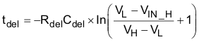
- Ability to accept slow dV/dt input signals, which allows designers to use RCD circuits on the input pin to program propagation delays in the application, as shown below:
 Figure 26. Using RCD Circuits
The UCC2752x devices feature an important safety feature, whenever any of the input pins is in a floating condition, the output of the respective channel is held in the low state. This is achieved using VDD pull-up resistors on all the inverting inputs (INA-, INB- in UCC27527) or GND pull-down resistors on all the non-inverting input pins (INA, INB in UCC27528 and INA+, INB+ in UCC27527), as shown in the device's block diagrams.
While UCC27528 features one input pin per channel, the UCC27527 features a dual input configuration with two input pins available to control the output state of each channel. With the UCC27527 device the user has the flexibility to drive each channel using either a non-inverting input pin (INx+) or an inverting input pin (INx-). The state of the output pin is dependent on the bias on both the INx+ and INx- pins (where x = A, B). Once an input pin has been chosen to drive a channel, the other input pin of that channel (the unused Input pin) must be properly biased in order to enable the output of the channel. The unused input pin cannot remain in a floating condition because, as mentioned earlier, whenever any input pin is left in a floating condition, the output of that channel is disabled using the internal pull-up and down resistors for safety purposes. Alternatively, the unused input pin can effectively be used to implement an enable and disable function, as explained below.
- In order to drive the channel “x” (x = A or B) in a non-inverting configuration, apply the PWM control input signal to INx+ pin. In this case, the unused input pin, INx-, must be biased low (eg. tied to GND) in order to enable the output of this channel.
- Alternately, the INx- pin can be used to implement the enable and disable function using an external logic signal. OUTx is disabled when INx- is biased high and OUTx is enabled when INX- is biased low.
- In order to drive the channel “X” (X = A or B) in an inverting configuration, apply the PWM control input signal to INX- pin. In this case, the unused input pin, INX+, must be biased high (eg. tied to VDD) in order to enable the output of the channel.
- Alternately, the INX+ pin can be used to implement the enable and disable function using an external logic signal. OUTX is disabled when INX+ is biased low and OUTX is enabled when INX+ is biased high.
- Finally, it is worth noting that the UCC27527 output pin can be driven into high state ONLY when INx+ pin is biased high AND INx- input is biased low.
Refer to the input and output logic truth table and typical application diagram for additional clarification.
8.3.4 Enable Function
The enable function is an extremely beneficial feature in gate driver devices especially for certain applications such as synchronous rectification where the driver outputs can be disabled in light-load conditions to prevent negative current circulation and to improve light-load efficiency.
UCC27528 device is provided with independent enable pins ENx for exclusive control of each driver channel operation. The enable pins are based on a non-inverting configuration (active high operation). Thus when ENx pins are driven high the drivers are enabled and when ENx pins are driven low the drivers are disabled. Like the input pins, the enable pins are also based on a TTL/CMOS compatible input threshold logic that is independent of the supply voltage and can be effectively controlled using logic signals from 3.3-V and 5-V microcontrollers. The UCC2752X devices also feature tight control of the Enable function threshold voltage levels which eases system design considerations and ensures stable operation across temperature (refer to Figure 10). The ENx pins are internally pulled up to VDD using pull-up resistors as a result of which the outputs of the device are enabled in the default state. Hence the ENx pins can be left floating or Not Connected (N/C) for standard operation, where the enable feature is not needed. Essentially, this allows the UCC27528 device to be pin-to-pin compatible with TI’s previous generation drivers UCC27323/4/5 respectively, where pins 1, 8 are N/C pins. If the channel A and Channel B inputs and outputs are connected in parallel to increase the driver current capacity, ENA and ENB should be connected and driven together.
The UCC27527 device does not feature dedicated enable pins. However, as mentioned earlier, an enable/disable function can be easily implemented in UCC27527 using the unused input pin. When INx+ is pulled-down to GND or INx- is pulled-down to VDD, the output is disabled. Thus INx+ pin can be used like an enable pin that is based on active high logic, while INx- can be used like an enable pin that is based on active low logic. It is important to note that while the ENA, ENB pins in the UCC27528 are allowed to be in floating condition during standard operation and the outputs will be enabled, the INx+, INx- pins in UCC27527 are not allowed to be floating since this will disable the outputs.
8.3.5 Output Stage
The UCC2752x device output stage features a unique architecture on the pull-up structure which delivers the highest peak Source current when it is most needed during the Miller plateau region of the power switch turn-on transition (when the power switch drain/collector voltage experiences dV/dt). The output stage pull-up structure features a P-Channel MOSFET and an additional N-Channel MOSFET in parallel. The function of the N-Channel MOSFET is to provide a brief boost in the peak sourcing current enabling fast turn-on. This is accomplished by briefly turning-on on the N-Channel MOSFET during a narrow instant when the output is changing state from Low to High.

The ROH parameter (see Electrical Characteristics) is a DC measurement and it is representative of the on-resistance of the P-Channel device only. This is because the N-Channel device is held in the off state in DC condition and is turned-on only for a narrow instant when output changes state from low to high. Thus it should be noted that effective resistance of UCC2752x pull-up stage during turn-on instant is much lower than what is represented by ROH parameter.
The pull-down structure in UCC2752x is simply composed of a N-Channel MOSFET. The ROL parameter (see Electrical Characteristics), which is also a DC measurement, is representative of the impedance of the pull-down stage in the device. In UCC2752x, the effective resistance of the hybrid pull-up structure during turn-on is estimated to be approximately 1.5 x ROL, estimated based on design considerations.
Each output stage in UCC2752x is capable of supplying 5-A peak source and 5-A peak sink current pulses. The output voltage swings between VDD and GND providing rail-to-rail operation, thanks to the MOS output stage which delivers very low drop-out. The presence of the MOSFET body diodes also offers low impedance to switching overshoots and undershoots. This means that in many cases, external Schottky diode clamps may be eliminated. The outputs of these drivers are designed to withstand 500-mA reverse current without either damage to the device or logic malfunction.
The UCC2752x devices are particularly suited for dual-polarity, symmetrical drive gate transformer applications where the primary winding of transformer driven by OUTA and OUTB, with inputs INA and INB being driven complementary to each other. This is due to the extremely low drop-out offered by the MOS output stage of these devices, both during high (VOH) and low (VOL) states along with the low impedance of the driver output stage, all of which allow alleviate concerns regarding transformer demagnetization and flux imbalance. The low propagation delays also ensure accurate reset for high-frequency applications.
For applications that have zero voltage switching during power MOSFET turn-on or turn-off interval, the driver supplies high-peak current for fast switching even though the miller plateau is not present. This situation often occurs in synchronous rectifier applications because the body diode is generally conducting before power MOSFET is switched on.
8.3.6 Low Propagation Delays and Tightly Matched Outputs
The UCC2752x driver devices offer a very low propagation delay of 17-ns (typical) between input and output which offers lowest level of pulse transmission distortion available in the industry for high-frequency switching applications. For example in synchronous rectifier applications, the SR MOSFETs can be driven with very low distortion when a single driver device is used to drive both the SR MOSFETs. Further, the driver devices also feature an extremely accurate, 1-ns (typ) matched internal propagation delays between the two channels which is beneficial for applications requiring dual gate drives with critical timing. For example in a PFC application, a pair of paralleled MOSFETs may be driven independently using each output channel, which the inputs of both channels are driven by a common control signal from the PFC controller device. In this case the 1-ns delay matching ensures that the paralleled MOSFETs are driven in a simultaneous fashion with the minimum of turn-on delay difference.
Since the CMOS input threshold of UCC27528 allows the use of slow dV/dt input signals, when paralleling outputs for obtaining higher peak output current capability, it is recommended to connect external gate resistors directly to the output pins to avoid shoot-through current conduction between the 2 channels, as shown in Figure 28. While the two channels are inherently very well matched (4-ns Max propagation delay), it should be noted that there may be differences in the input threshold voltage level between the two channels or differences in the input signals which can cause the delay between the two outputs.
 Figure 28. Slow Input Signal May Cause Shoot-Through Between Channels During Paralleling
8.4 Device Functional Modes
The device operates in normal mode and UVLO mode. See the VDD and Undervoltage Lockout section for information on UVLO operation mode. In the normal mode the output state is dependent on states of the IN+ and IN– pins. Table 2 and Table 3 lists the output states for different input pin combinations.