SLUSD37E October   2017  – November 2019 UCC28056

PRODUCTION DATA.  

  1. Features
  2. Applications
  3. Description
    1.     No Load Power
      1.      Device Images
        1.       Simplified Application
  4. Revision History
  5. Device Comparison Tables
  6. Pin Configuration and Functions
    1.     Pin Functions
  7. Specifications
    1. 7.1 Absolute Maximum Ratings
    2. 7.2 ESD Ratings
    3. 7.3 Recommended Operating Conditions
    4. 7.4 Thermal Information
    5. 7.5 Electrical Characteristics
    6. 7.6 Typical Characteristics
  8. Detailed Description
    1. 8.1 Overview
    2. 8.2 Functional Block Diagram
    3. 8.3 Feature Description
      1. 8.3.1 CrM/DCM Control Principle
      2. 8.3.2 Line Voltage Feed-Forward
        1. 8.3.2.1 Peak Line Voltage Detection
      3. 8.3.3 Valley Switching and CrM/DCM Hysteresis
        1. 8.3.3.1 Valley Delay Adjustment
      4. 8.3.4 Transconductance Amplifier with Transient Speed-up Function
      5. 8.3.5 Faults and Protections
        1. 8.3.5.1 Supply Undervoltage Lockout
        2. 8.3.5.2 Two Level Over-Current Protection
          1. 8.3.5.2.1 Cycle-by-Cycle Current Limit Ocp1
          2. 8.3.5.2.2 Ocp2 Gross Over-Current or CCM Protection
        3. 8.3.5.3 Output Over-Voltage Protection
          1. 8.3.5.3.1 First Level Output Over-Voltage Protection (Ovp1)
          2. 8.3.5.3.2 Second Level Over-Voltage Protection (Ovp2)
        4. 8.3.5.4 Thermal Shutdown Protection
        5. 8.3.5.5 Line Under-Voltage or Brown-In
      6. 8.3.6 High-Current Driver
    4. 8.4 Controller Functional Modes
      1. 8.4.1 Burst Mode Operation
      2. 8.4.2 Soft Start
  9. Application and Implementation
    1. 9.1 Application Information
    2. 9.2 Typical Application
      1. 9.2.1 Design Requirements
      2. 9.2.2 Detailed Design Procedure
        1. 9.2.2.1 Custom Design With WEBENCH® Tools
        2. 9.2.2.2 Power Stage Design
          1. 9.2.2.2.1 Boost Inductor Design
          2. 9.2.2.2.2 Boost Switch Selection
          3. 9.2.2.2.3 Boost Diode Selection
          4. 9.2.2.2.4 Output Capacitor Selection
        3. 9.2.2.3 ZCD/CS Pin
          1. 9.2.2.3.1 Voltage Spikes on the ZCD/CS pin Waveform
        4. 9.2.2.4 VOSNS Pin
        5. 9.2.2.5 Voltage Loop Compensation
          1. 9.2.2.5.1 Plant Model
          2. 9.2.2.5.2 Compensator Design
      3. 9.2.3 Application Curves
  10. 10Power Supply Recommendations
  11. 11Layout
    1. 11.1 Layout Guidelines
      1. 11.1.1 VOSNS Pin
      2. 11.1.2 ZCD/CS Pin
      3. 11.1.3 VCC Pin
      4. 11.1.4 GND Pin
      5. 11.1.5 DRV Pin
      6. 11.1.6 COMP Pin
    2. 11.2 Layout Example
  12. 12Device and Documentation Support
    1. 12.1 Custom Design With WEBENCH® Tools
    2. 12.2 Receiving Notification of Documentation Updates
    3. 12.3 Community Resources
    4. 12.4 Trademarks
    5. 12.5 Electrostatic Discharge Caution
    6. 12.6 Glossary
  13. 13Mechanical, Packaging, and Orderable Information

Package Options

Mechanical Data (Package|Pins)
Thermal pad, mechanical data (Package|Pins)
Orderable Information

Description

The UCC28056 device drives PFC boost stages based on an innovative mixed mode method that operates in transition mode (TM) at full load and transitions seamlessly into discontinuous conduction mode (DCM) at reduced load, automatically reducing switching frequency. This device incorporates burst mode operation to further improve light load performance, enabling systems to meet challenging energy standards while eliminating the need to switch off the PFC. UCC28056 can drive a PFC power stage up to 300 W, ensuring sinusoidal line input current with low distortion, close to unity power factor. When used with the LLC controller UCC256403/4, and dual synchronous rectifier controller UCC24624 less than 80 mW system standby power can be achieved, enabling PFC always on architecture and eliminating the need for an auxiliary converter. This with FET Drain valley turn-on with simple boost inductor allows fewest component count and reduced system cost.

Device Information(1)

PART NUMBER PACKAGE BODY SIZE (NOM)
UCC28056 SOT-23(6) 2.90 mm x 1.6 mm
  1. For all available packages, see the orderable addendum at the end of the data sheet.

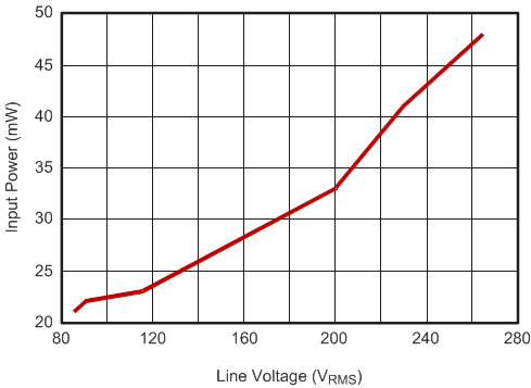
No Load Power
UCC28056 fp_line_power_slusd37.gif