SLUS577D November   2011  – August 2016 UCC2817A , UCC2818A , UCC3817A , UCC3818A

PRODUCTION DATA.  

  1. Features
  2. Applications
  3. Description
  4. Revision
  5. Description (Continued)
  6. Device Comparison Tables
  7. Pin Configuration and Functions
  8. Specifications
    1. 8.1 Absolute Maximum Ratings
    2. 8.2 ESD Ratings
    3. 8.3 Recommended Operating Conditions
    4. 8.4 Thermal Information
    5. 8.5 Electrical Characteristics
    6. 8.6 Typical Characteristics
  9. Detailed Description
    1. 9.1 Overview
    2. 9.2 Functional Block Diagram
    3. 9.3 Feature Description
      1. 9.3.1 Reference Section and Error Amplifier
      2. 9.3.2 Zero Power Block
      3. 9.3.3 Multiplier
      4. 9.3.4 Output Overvoltage Protection
      5. 9.3.5 Pin Descriptions
        1. 9.3.5.1  CAI
        2. 9.3.5.2  CAOUT
        3. 9.3.5.3  CT
        4. 9.3.5.4  DRVOUT
        5. 9.3.5.5  GND
        6. 9.3.5.6  IAC
        7. 9.3.5.7  MOUT
        8. 9.3.5.8  OVP/EN
        9. 9.3.5.9  PKLMT
        10. 9.3.5.10 RT
        11. 9.3.5.11 SS
        12. 9.3.5.12 VAOUT
        13. 9.3.5.13 VCC
        14. 9.3.5.14 VFF
        15. 9.3.5.15 VSENSE
        16. 9.3.5.16 VREF
    4. 9.4 Device Functional Modes
      1. 9.4.1 Transition Mode Control
  10. 10Application and Implementation
    1. 10.1 Application Information
    2. 10.2 Typical Application
      1. 10.2.1 Design Requirements
      2. 10.2.2 Detailed Design Procedure
        1. 10.2.2.1 Power Stage
          1. 10.2.2.1.1 LBOOST
          2. 10.2.2.1.2 COUT
          3. 10.2.2.1.3 Power Switch Selection
        2. 10.2.2.2 Soft Start
        3. 10.2.2.3 Multiplier
        4. 10.2.2.4 Voltage Loop
        5. 10.2.2.5 Current Loop
        6. 10.2.2.6 Start-Up
        7. 10.2.2.7 Capacitor Ripple Reduction
      3. 10.2.3 Application Curves
  11. 11Power Supply Recommendations
  12. 12Layout
    1. 12.1 Layout Guidelines
      1. 12.1.1 Bias Current
      2. 12.1.2 VREF
    2. 12.2 Layout Example
  13. 13Device and Documentation Support
    1. 13.1 Documentation Support
      1. 13.1.1 Related Documentation
    2. 13.2 Related Links
    3. 13.3 Receiving Notification of Documentation Updates
    4. 13.4 Community Resource
    5. 13.5 Trademarks
    6. 13.6 Electrostatic Discharge Caution
    7. 13.7 Glossary
  14. 14Mechanical, Packaging, and Orderable Information

Package Options

Refer to the PDF data sheet for device specific package drawings

Mechanical Data (Package|Pins)
  • PW|16
  • N|16
  • D|16
Thermal pad, mechanical data (Package|Pins)
Orderable Information

12 Layout

12.1 Layout Guidelines

12.1.1 Bias Current

The bias voltage is supplied either by an external dedicated DC-DC converter or by an auxiliary winding from the PFC inductor or the 2nd stage DC-DC converter.

The bias capacitor should be large enough to maintain sufficient voltage with AC line variations. Connect a 1-µF capacitor between VCC and GND as close to the IC as possible. For wide line voltages, an additional 18-V Zener clamp can also be used.

12.1.2 VREF

Connect a capacitor >=0.1 µF between VREF and GND for stability.

12.2 Layout Example
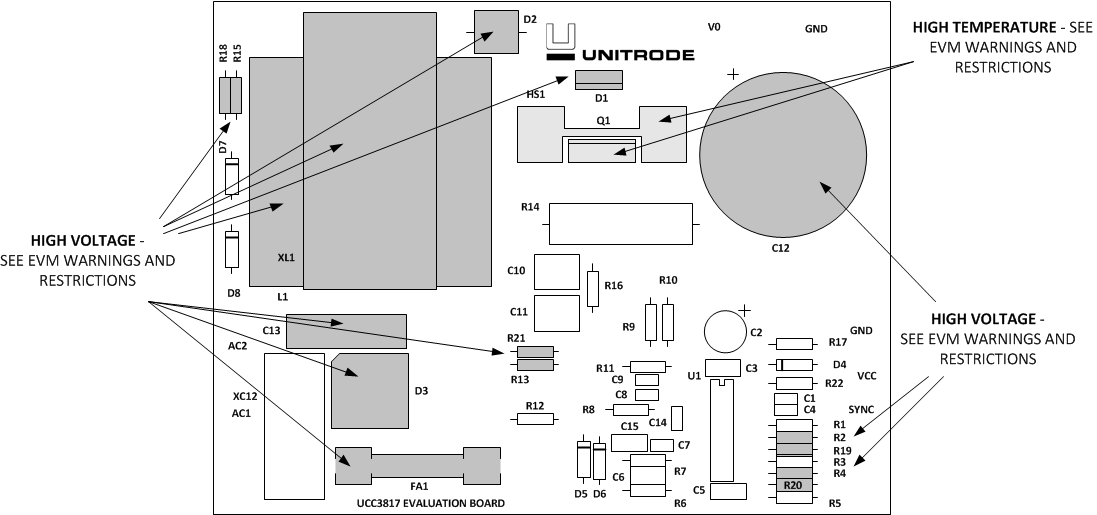
UCC2817A UCC2818A UCC3817A UCC3818A fig2_sluu077.gif Figure 17. UCC3817EVM Evaluation Board Layout Assembly