SLUS492K June 2001 – November 2023 UCC27323 , UCC27324 , UCC27325 , UCC37323 , UCC37324 , UCC37325
PRODUCTION DATA
- 1
- 1 Features
- 2 Applications
- 3 Description
- 4 Device Comparison Table
- 5 Pin Configuration and Functions
- 6 Specifications
- 7 Detailed Description
- 8 Application and Implementation
- 9 Power Supply Recommendations
- 10Layout
- 11Device and Documentation Support
- 12Revision History
- 13Mechanical, Packaging, and Orderable Information
Package Options
Mechanical Data (Package|Pins)
Thermal pad, mechanical data (Package|Pins)
- DGN|8
Orderable Information
3 Description
The UCC2732x and UCC3732x family of high-speed dual-MOSFET Drivers deliver 4-A source and 4-A sink peak current to effectively drive MOSFETs where it is needed most at the Miller Plateau Region. A unique BiPolar and MOSFET hybrid output stage in parallel also allows efficient current sourcing and sinking at low supply voltages. Three standard logic options are offered — dual-inverting, dual-noninverting, and one-inverting and one-noninverting driver. Input thresholds are based on TTL and CMOS and independent of supply voltage and feature wide input hysteresis offering excellent noise immunity. The UCC2732x and UCC3732x family is available in the standard SOIC-8 (D) as well as the thermally enhanced -8pin PowerPAD MSOP package (DGN), drastically lowering thermal resistance to improve long term reliability.
| DEVICE(1) | KEY SPECS | PACKAGE |
|---|---|---|
| UCCx732x | -40C <= Temp <= 125C 4.5V <= VDD<= 15V 20ns/15ns - Rise/Fall times @ 1.8nF load 35ns/25ns Rise/Fall Prop Delay | SOIC (8): 4.90 mm × 3.91 mm |
| MSOP-PowerPAD (8): 3.00 mm × 3.00 mm |
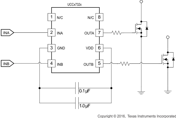
 Simplified Application Diagram