SLUS577D November 2011 – August 2016 UCC2817A , UCC2818A , UCC3817A , UCC3818A
PRODUCTION DATA.
- 1 Features
- 2 Applications
- 3 Description
- 4 Revision
- 5 Description (Continued)
- 6 Device Comparison Tables
- 7 Pin Configuration and Functions
- 8 Specifications
- 9 Detailed Description
- 10Application and Implementation
- 11Power Supply Recommendations
- 12Layout
- 13Device and Documentation Support
- 14Mechanical, Packaging, and Orderable Information
Package Options
Refer to the PDF data sheet for device specific package drawings
Mechanical Data (Package|Pins)
- N|16
- D|16
Thermal pad, mechanical data (Package|Pins)
- D|16
Orderable Information
10 Application and Implementation
NOTE
Information in the following applications sections is not part of the TI component specification, and TI does not warrant its accuracy or completeness. TI’s customers are responsible for determining suitability of components for their purposes. Customers should validate and test their design implementation to confirm system functionality.
10.1 Application Information
The UCC3817A is a BiCMOS average current mode boost controller for high power factor, high efficiency preregulator power supplies. Figure 5 shows the UCC3817A in a 250-W PFC preregulator circuit. Off-line switching power converters normally have an input current that is not sinusoidal. The input current waveform has a high harmonic content because current is drawn in pulses at the peaks of the input voltage waveform. An active power factor correction circuit programs the input current to follow the line voltage, forcing the converter to look like a resistive load to the line. A resistive load has 05 phase displacement between the current and voltage waveforms. Power factor can be defined in terms of the phase angle between two sinusoidal waveforms of the same frequency:

Therefore, a purely resistive load would have a power factor of 1. In practice, power factors of 0.999 with THD (total harmonic distortion) of less than 3% are possible with a well-designed circuit. See the following guidelines for designing PFC boost converters using the UCC3817A.
NOTE
Schottky diodes, D5 and D6, are required to protect the PFC controller from electrical over stress during system power up.
10.2 Typical Application
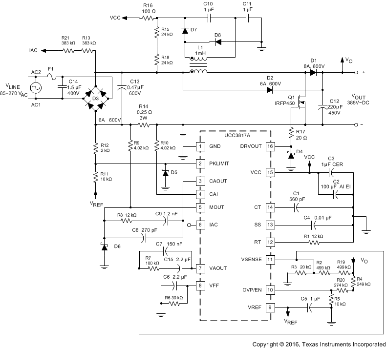 Figure 5. Typical Application Circuit
10.2.1 Design Requirements
Table 3 lists the parameters for this application.
Table 3. Design Parameters
| PARAMETER | TEST CONDITIONS | MIN | TYP | MAX | UNIT | ||
|---|---|---|---|---|---|---|---|
| VIN | Input RMS voltage | 85 | 270 | V | |||
| Input frequency | 50/60 | Hz | |||||
| VOUT | Output Voltage | 385 | 420 | V | |||
| POUT | Output Power | 250 | W | ||||
| Holdup Time | All line and load conditions | 16 | ms | ||||
| Efficiency | Efficiency at 85 Vrms, 100% Load | 91% | |||||
| THD at Low Line | 85 Vrms = 100% Load | 5% | |||||
| THD at High Line | 265 Vrms, 100% Load | 15% | |||||
10.2.2 Detailed Design Procedure
10.2.2.1 Power Stage
10.2.2.1.1 LBOOST
The boost inductor value is determined by Equation 6:

where D is the duty cycle, DI is the inductor ripple current and fS is the switching frequency. For the example circuit a switching frequency of 100 kHz, a ripple current of 875 mA, a maximum duty cycle of 0.688 and a minimum input voltage of 85 VRMS gives us a boost inductor value of about 1 mH. The values used in this equation are at the peak of low line, where the inductor current and its ripple are at a maximum.
10.2.2.1.2 COUT
Two main criteria, the capacitance and the voltage rating, dictate the selection of the output capacitor. The value of capacitance is determined by the holdup time required for supporting the load after input ac voltage is removed. Holdup is the amount of time that the output stays in regulation after the input has been removed. For this circuit, the desired holdup time is approximately 16 ms. Expressing the capacitor value in terms of output power, output voltage, and holdup time gives Equation 7:

In practice, the calculated minimum capacitor value may be inadequate because output ripple voltage specifications limit the amount of allowable output capacitor ESR. Attaining a sufficiently low value of ESR often necessitates the use of a much larger capacitor value than calculated. The amount of output capacitor ESR allowed can be determined by dividing the maximum specified output ripple voltage by the inductor ripple current. In this design holdup time was the dominant determining factor and a 220-µF, 450-V capacitor was chosen for the output voltage level of 385 VDC at 250 W.
10.2.2.1.3 Power Switch Selection
As in any power supply design, tradeoffs between performance, cost and size have to be made. When selecting a power switch, it can be useful to calculate the total power dissipation in the switch for several different devices at the switching frequencies being considered for the converter. Total power dissipation in the switch is the sum of switching loss and conduction loss. Switching losses are the combination of the gate charge loss, COSS loss and turnon and turnoff losses, as shown in Equation 8, Equation 9, and Equation 10.


where
- QGATE is the total gate charge
- VGATE is the gate drive voltage
- fS is the clock frequency
- COSS is the drain source capacitance of the MOSFET
- IL is the peak inductor current
- tON and tOFF are the switching times (estimated using device parameters RGATE
- QGD and VTH) and VOFF is the voltage across the switch during the off time, in this case VOFF = VOUT
Conduction loss is calculated with Equation 11 as the product of the RDS(on) of the switch (at the worst case junction temperature) and the square of RMS current:

where
- K is the temperature factor found in the manufacturer's RDS(on) vs. junction temperature curves
Calculating these losses and plotting against frequency gives a curve that enables the designer to determine either which manufacturer's device has the best performance at the desired switching frequency, or which switching frequency has the least total loss for a particular power switch. For this design example an IRFP450 HEXFET from International Rectifier was chosen because of its low RDS(on) and its VDSS rating. The IRFP450's RDS(on) of 0.4 Ω and the maximum VDSS of 500 V made it an ideal choice. An excellent review of this procedure can be found in the Unitrode Power Supply Design Seminar SEM1200, Topic 6, Design Review: 140 W, [Multiple Output High Density DC/DC Converter].
10.2.2.2 Soft Start
The soft-start circuitry is used to prevent overshoot of the output voltage during start-up. This is accomplished by bringing up the voltage amplifier's output (VVAOUT) slowly which allows for the PWM duty cycle to increase slowly. Use the following equation to select a capacitor for the soft-start pin.
In this example tDELAY is equal to 7.5 ms, which would yield a CSS of 10 nF.

In an open-loop test circuit, shorting the soft-start pin to ground does not ensure 0% duty cycle. This is due to the current amplifiers input offset voltage, which could force the current amplifier output high or low depending on the polarity of the offset voltage. However, in the typical application there is sufficient amount of inrush and bias current to overcome the current amplifier's offset voltage.
10.2.2.3 Multiplier
The output of the multiplier of the UCC3817A is a signal representing the desired input line current. It is an input to the current amplifier, which programs the current loop to control the input current to give high power factor operation. As such, the proper functioning of the multiplier is key to the success of the design. The inputs to the multiplier are VAOUT, the voltage amplifier error signal, IIAC, a representation of the input rectified ac line voltage, and an input voltage feedforward signal, VVFF. The output of the multiplier, IMOUT, can be expressed as shown in Equation 13.

where
- K is a constant typically equal to 1 / V.
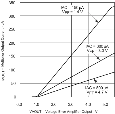
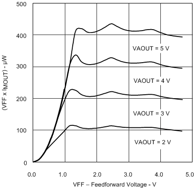
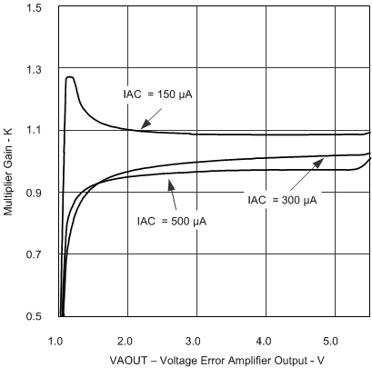
The Electrical Characteristics table covers all the required operating conditions for designing with the multiplier. Additionally, curves in Figure 14, Figure 15, and Figure 16 provide typical multiplier characteristics over its entire operating range.
The IIAC signal is obtained through a high-value resistor connected between the rectified ac line and the IAC pin of the UCC3817A and UCC3818A. This resistor (RIAC) is sized to give the maximum IIAC current at high line. For the UCC3817A and UCC3818A the maximum IIAC current is about 500 mA. A higher current than this can drive the multiplier out of its linear range. A smaller current level is functional, but noise can become an issue, especially at low input line. Assuming a universal line operation of 85 VRMS to 265 VRMS gives a RIAC value of 750 kΩ. Because of voltage rating constraints of standard 1/4-W resistor, use a combination of lower value resistors connected in series to give the required resistance and distribute the high voltage amongst the resistors. For this design example two 383-kΩ resistors were used in series.
The current into the IAC pin is mirrored internally to the VFF pin where it is filtered to produce a voltage feed forward signal proportional to line voltage. The VFF voltage is used to keep the power stage gain constant; and to provide input power limiting. See Texas Instruments application note Unitrode - UC3854A/B and UC3855A/B Provide Power Limiting With Sinusoidal Input Current for PFC Front Ends (SLUA196) for a detailed explanation on how the VFF pin provides power limiting. Equation 14 can be used to size the VFF resistor (RVFF) to provide power limiting where VIN(min) is the minimum RMS input voltage and RIAC is the total resistance connected between the IAC pin and the rectified line voltage.

Because the VFF voltage is generated from line voltage it needs to be adequately filtered to reduce total harmonic distortion caused by the 120 Hz rectified line voltage. Refer to the Unitrode Power Supply Design Seminar, SEM-700 Topic 7, [Optimizing the Design of a High Power Factor Preregulator.] A single pole filter was adequate for this design. Assuming that an allocation of 1.5% total harmonic distortion from this input is allowed, and that the second harmonic ripple is 66% of the input ac line voltage, the amount of attenuation required by this filter is:

With a ripple frequency (fR) of 120 Hz and an attenuation of 0.022 requires that the pole of the filter (fP) be placed at:

Equation 17 can be used to select the filter capacitor (CVFF) required to produce the desired low pass filter.

The RMOUT resistor is sized to match the maximum current through the sense resistor to the maximum multiplier current. The maximum multiplier current, or IMOUT(max), can be determined by Equation 18:

IMOUT(max) for this design is approximately 315 mA. The RMOUT resistor can then be determined by Equation 19:

In this example VRSENSE was selected to give a dynamic operating range of 1.25 V, which gives an RMOUT of roughly 3.91 kΩ.
10.2.2.4 Voltage Loop
The second major source of harmonic distortion is the ripple on the output capacitor at the second harmonic of the line frequency. This ripple is fed back through the error amplifier and appears as a 3rd harmonic ripple at the input to the multiplier. The voltage loop must be compensated not just for stability but also to attenuate the contribution of this ripple to the total harmonic distortion of the system (see Figure 6).
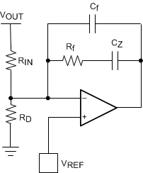 Figure 6. Voltage Amplifier Configuration
The gain of the voltage amplifier, GVA, can be determined by first calculating the amount of ripple present on the output capacitor. The peak value of the second harmonic voltage is given by Equation 20.

In this example VOPK is equal to 3.91 V. Assuming an allowable contribution of 0.75% (1.5% peak to peak) from the voltage loop to the total harmonic distortion budget we set the gain equal to Equation 21.

where
- ΔVVAOUT is the effective output voltage range of the error amplifier (5 V for the UCC3817A).
The network needed to realize this filter is comprised of an input resistor, RIN, and feedback components Cf, CZ, and Rf. The value of RIN is already determined because of its function as one half of a resistor divider from VOUT feeding back to the voltage amplifier for output voltage regulation. In this case the value was chosen to be 1 MΩ. This high value was chosen to reduce power dissipation in the resistor. In practice, the resistor value would be realized by the use of two 500-kΩ resistors in series because of the voltage rating constraints of most standard 1/4-W resistors. The value of Cf is determined by Equation 22.

In this example Cf equals 150 nF. Resistor Rf sets the dc gain of the error amplifier and thus determines the frequency of the pole of the error amplifier. The location of the pole can be found by setting the gain of the loop equation to one and solving for the crossover frequency. The frequency, expressed in terms of input power, can be calculated by Equation 23.

fVI for this converter is 10 Hz. A derivation of this equation can be found in the Unitrode Power Supply Design Seminar SEM1000, Topic 1, [A 250-kHz, 500-W Power Factor Correction Circuit Employing Zero Voltage Transitions].
Solving for Rf becomes Equation 24.

or Rf equals 100 kΩ.
Due to the low output impedance of the voltage amplifier, capacitor CZ was added in series with RF to reduce loading on the voltage divider. To ensure the voltage loop crossed over at fVI, CZ was selected to add a zero at a 10th of fVI. For this design, a 2.2-µF capacitor was chosen for CZ. Equation 25 can be used to calculate CZ.

10.2.2.5 Current Loop
The gain of the power stage is calculated by Equation 26.

RSENSE has been chosen to give the desired differential voltage for the current sense amplifier at the desired current limit point. In this example, a current limit of 4 A and a reasonable differential voltage to the current amp of 1 V gives a RSENSE value of 0.25 Ω. VP in Equation 26 is the voltage swing of the oscillator ramp, 4 V for the UCC3817A. Setting the crossover frequency of the system to 1/10th of the switching frequency, or 10 kHz, requires a power stage gain at that frequency of 0.383. For the system to have a gain of 1 at the crossover frequency, the current amplifier needs to have a gain of 1/GID at that frequency. GEA, the current amplifier gain is then:

RI is the RMOUT resistor, previously calculated to be 3.9 kΩ. (see Figure 7). The gain of the current amplifier is Rf/RI, so multiplying RI by GEA gives the value of Rf, in this case approximately 12 kΩ. Setting a zero at the crossover frequency and a pole at half the switching frequency completes the current loop compensation.


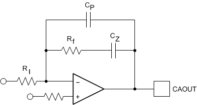 Figure 7. Current Loop Compensation
The UCC3817A current amplifier has the input from the multiplier applied to the inverting input. This change in architecture from previous Texas Instruments PFC controllers improves noise immunity in the current amplifier. It also adds a phase inversion into the control loop. The UCC3817A takes advantage of this phase inversion to implement leading-edge duty cycle modulation. Synchronizing a boost PFC controller to a downstream dc-to-dc controller reduces the ripple current seen by the bulk capacitor between stages, reducing capacitor size and cost and reducing EMI. This is explained in greater detail in the following section. The UCC3817A current amplifier configuration is shown in Figure 8.
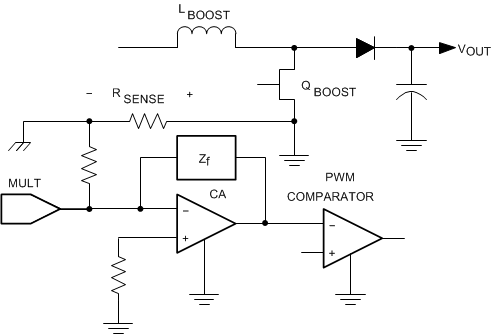 Figure 8. UCC3817A Current Amplifier Configuration
10.2.2.6 Start-Up
The UCC3818A version of the device is intended to have VCC connected to a 12-V supply voltage. The UCC3817A has an internal shunt regulator enabling the device to be powered from bootstrap circuitry as shown in the typical application circuit of Figure 5. The current drawn by the UCC3817A during undervoltage lockout, or start-up current, is typically 150 µA. Once VCC is above the UVLO threshold, the device is enabled and draws 4 mA typically. A resistor connected between the rectified ac line voltage and the VCC pin provides current to the shunt regulator during power up. Once the circuit is operational, the bootstrap winding of the inductor provides the VCC voltage. Sizing of the start-up resistor is determined by the start-up time requirement of the system design.


where
- IC is the charge current
- C is the total capacitance at the VCC pin
- ΔV is the UVLO threshold and Δt is the allowed start-up time
Assuming a 1 second allowed start-up time, a 16-V UVLO threshold, and a total VCC capacitance of 100 µF, a resistor value of 51 kΩ is required at a low line input voltage of 85 VRMS. The IC start-up current is sufficiently small as to be ignored in sizing the start-up resistor.
10.2.2.7 Capacitor Ripple Reduction
For a power system where the PFC boost converter is followed by a dc-to-dc converter stage, there are benefits to synchronizing the two converters. In addition to the usual advantages such as noise reduction and stability, proper synchronization can significantly reduce the ripple currents in the boost circuit's output capacitor. Figure 9 helps illustrate the impact of proper synchronization by showing a PFC boost converter together with the simplified input stage of a forward converter. The capacitor current during a single switching cycle depends on the status of the switches Q1 and Q2 and is shown in Figure 10. It can be seen that with a synchronization scheme that maintains conventional trailing-edge modulation on both converters, the capacitor current ripple is highest. The greatest ripple current cancellation is attained when the overlap of Q1 off-time and Q2 on-time is maximized. One method of achieving this is to synchronize the turnon of the boost diode (D1) with the turnon of Q2. This approach implies that the boost converter's leading edge is pulse width modulated while the forward converter is modulated with traditional trailing edge PWM. The UCC3817A is designed as a leading edge modulator with easy synchronization to the downstream converter to facilitate this advantage. Table 4 compares the ICB(rms) for D1/Q2 synchronization as offered by UCC3817A vs the ICB(rms) for the other extreme of synchronizing the turnon of Q1 and Q2 for a 200-W power system with a VBST of 385 V.
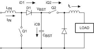 Figure 9. Simplified Representation of a 2-Stage PFC Power Supply
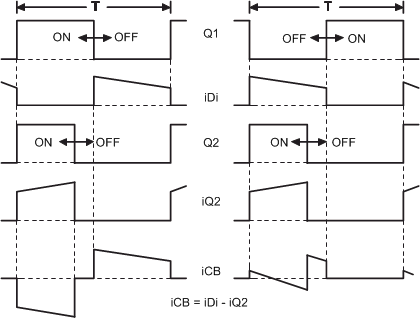 Figure 10. Timing Waveforms for Synchronization Scheme
Table 4 illustrates that the boost capacitor ripple current can be reduced by about 50% at nominal line and about 30% at high line with the synchronization scheme facilitated by the UCC3817A. Figure 11 shows the suggested technique for synchronizing the UCC3817A to the downstream converter. With this technique, maximum ripple reduction as shown in Figure 10 is achievable. The output capacitance value can be significantly reduced if its choice is dictated by ripple current or the capacitor life can be increased as a result. In cost sensitive designs where holdup time is not critical, this is a significant advantage.
Table 4. Effects of Synchronization on Boost Capacitor Current
| VIN = 85 V | VIN = 120 V | VIN = 240 V | ||||
|---|---|---|---|---|---|---|
| D(Q2) | Q1/Q2 | D1/Q2 | Q1/Q2 | D1/Q2 | Q1/Q2 | D1/Q2 |
| 0.35 | 1.491 A | 0.835 A | 1.341 A | 0.663 A | 1.024 A | 0.731 A |
| 0.45 | 1.432A | 0.93 A | 1.276 A | 0.664 A | 0.897 A | 0.614 A |
An alternative method of synchronization to achieve the same ripple reduction is possible. In this method, the turnon of Q1 is synchronized to the turnoff of Q2. While this method yields almost identical ripple reduction and maintains trailing edge modulation on both converters, the synchronization is much more difficult to achieve and the circuit can become susceptible to noise as the synchronizing edge itself is being modulated.
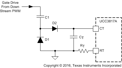 Figure 11. Synchronizing the UCC3817A to a Down-Stream Converter
10.2.3 Application Curves
