SLUS395K February 2000 – October 2015 UCC2817 , UCC2818 , UCC3817 , UCC3818
PRODUCTION DATA.
- 1 Features
- 2 Applications
- 3 Description
- 4 Revision History
- 5 Pin Configuration and Functions
- 6 Specifications
- 7 Detailed Description
- 8 Application and Implementation
- 9 Power Supply Recommendations
- 10Layout
- 11Device and Documentation Support
- 12Mechanical, Packaging, and Orderable Information
Package Options
Refer to the PDF data sheet for device specific package drawings
Mechanical Data (Package|Pins)
- PW|16
- DW|16
- N|16
- D|16
Thermal pad, mechanical data (Package|Pins)
Orderable Information
8 Application and Implementation
NOTE
Information in the following applications sections is not part of the TI component specification, and TI does not warrant its accuracy or completeness. TI’s customers are responsible for determining suitability of components for their purposes. Customers should validate and test their design implementation to confirm system functionality.
8.1 Application Information
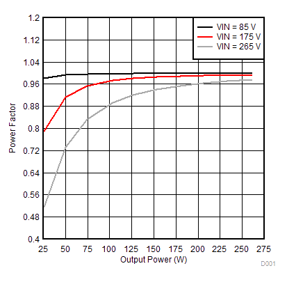
The UCC3817 is a BiCMOS average current mode boost controller for high power factor, high efficiency preregulator power supplies. Figure 9 shows the UCC3817 in a 250-W PFC preregulator circuit. Off-line switching power converters normally have an input current that is not sinusoidal. The input current waveform has a high harmonic content because current is drawn in pulses at the peaks of the input voltage waveform. An active power-factor correction circuit programs the input current to follow the line voltage, forcing the converter to look like a resistive load to the line. A resistive load has 0° phase displacement between the current and voltage waveforms. Power factor can be defined in terms of the phase angle between two sinusoidal waveforms of the same frequency:
PF = cos θ
Therefore, a purely resistive load would have a power factor of 1. In practice, power factors of 0.999 with THD (total harmonic distortion) of less than 3% are possible with a well-designed circuit. The following guidelines are provided to design PFC boost converters using the UCC3817.
NOTE
Schottky diodes, D5 and D6, are required to protect the PFC controller from electrical over stress during system power up.
8.2 Typical Application
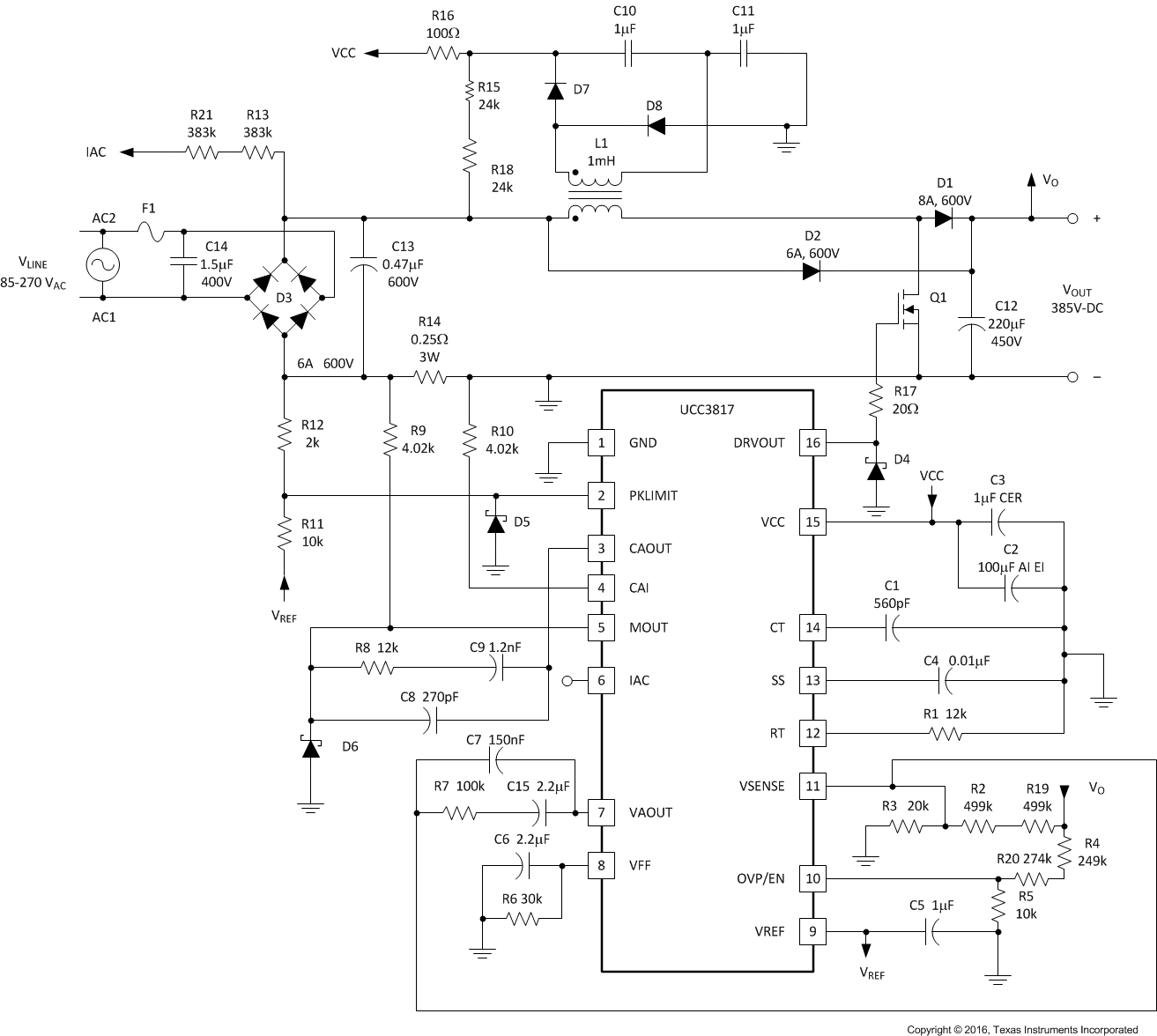 Figure 9. Typical Application Circuit
8.2.1 Design Requirements
Table 1 lists the parameters for this application.
Table 1. Design Parameters
| PARAMETER | TEST CONDITIONS | MIN | TYP | MAX | UNIT | ||
|---|---|---|---|---|---|---|---|
| VIN | Input RMS voltage | 85 | 270 | V | |||
| Input frequency | 50/60 | Hz | |||||
| VOUT | Output Voltage | 385 | 420 | V | |||
| POUT | Output Power | 250 | W | ||||
| Holdup Time | All line and load conditions | 16 | ms | ||||
| Efficiency | Efficiency at 85 Vrms, 100% Load | 91% | |||||
| THD at Low Line | 85 Vrms = 100% Load | 5% | |||||
| THD at High Line | 265 Vrms, 100% Load | 15% | |||||
8.2.2 Detailed Design Procedure
8.2.2.1 Power Stage
8.2.2.1.1 LBOOST
The boost inductor value is determined by:

where
- D is the duty cycle
- ΔI is the inductor ripple current
- fS is the switching frequency
For the example circuit in Figure 9, a switching frequency of 100 kHz, a ripple current of 875 mA, a maximum duty cycle of 0.688, and a minimum input voltage of 85 VRMS give a boost inductor value of approximately 1 mH. The values used in this equation are at the peak of low line, where the inductor current and its ripple are at a maximum.
8.2.2.1.2 COUT
Two main criteria, the capacitance and the voltage rating, dictate the selection of the output capacitor. The value of capacitance is determined by the holdup time required for supporting the load after input ac voltage is removed. Holdup is the amount of time that the output stays in regulation after the input has been removed. For the circuit in Figure 9, the desired holdup time is approximately 16 ms. Expressing the capacitor value in terms of output power, output voltage, and holdup time gives the equation:

In practice, the calculated minimum capacitor value may be inadequate, because output ripple voltage specifications limit the amount of allowable output capacitor ESR. Attaining a sufficiently low value of ESR often requires the use of a much larger capacitor value than calculated. The amount of output capacitor ESR allowed is determined by dividing the maximum specified output ripple voltage by the inductor ripple current. In the design in Figure 9, holdup time is the dominant determining factor, and a 220-μF, 450-V capacitor was chosen for the output voltage level of 385 VDC at 250 W.
8.2.2.2 Softstart
The softstart circuitry prevents overshoot of the output voltage during start up by bringing up the voltage amplifier output (VVAOUT) slowly, which allows for the PWM duty cycle to increase slowly. Use the following equation to select a capacitor for the softstart pin.
In this example, tDELAY is equal to 7.5 ms, which would yield a CSS of 10 nF.

In an open-loop test circuit, shorting the softstart pin to ground does not ensure 0% duty cycle. This is due to the input offset voltage of the current amplifier, which could force the current amplifier output high or low depending on the polarity of the offset voltage. However, in the typical application there is sufficient amount of inrush and bias current to overcome the offset voltage of the current amplifier.
8.2.2.3 Multiplier
The output of the multiplier of the UCC3817 is a signal representing the desired input line current. The multiplier is an input to the current amplifier, which programs the current loop to control the input current to give high power factor operation. As such, the proper functioning of the multiplier is key to the success of the design. The inputs to the multiplier are VAOUT, the voltage amplifier error signal, IIAC, a representation of the input rectified ac line voltage, and an input voltage feedforward signal, VVFF. The output of the multiplier, IMOUT, can be expressed as:

where
- K is a constant typically equal to 1/V
Electrical Characteristics covers all the required operating conditions for designing with the multiplier. Additionally, Figure 3, Figure 4, and Figure 5 provide typical multiplier characteristics over its entire operating range.
The IIAC signal is obtained through a high-value resistor connected between the rectified ac line and the IAC pin of the UCC381x. This resistor (RIAC) is sized to give the maximum IIAC current at high line. For the UCC381x, the maximum IIAC current is approximately 500 μA. A higher current than this can drive the multiplier out of its linear range. A smaller current level is functional, but noise can become an issue, especially at low input line. Assuming a universal line operation of 85 VRMS to 265 VRMS gives an RIAC value of 750 kΩ. Because of voltage rating constraints of standard 1/4-W resistor, use a combination of lower value resistors connected in series to give the required resistance and distribute the high voltage amongst the resistors. For the design example in Figure 9, two 383-kΩ resistors are used in series.
The current into the IAC pin is mirrored internally to the VFF pin, where it is filtered to produce a voltage feed forward signal proportional to line voltage. The VFF voltage keeps the power stage gain constant, and to provide input power limiting. Refer to Texas Instruments application note DN-66 UC3854A/B and UC3855A/B Provide Power Limiting with Sinusoidal Input (SLUA196) for detailed explanation on how the VFF pin provides power limiting. The following equation can be used to size the VFF resistor (RVFF) to provide power limiting where VIN(min) is the minimum RMS input voltage, and RIAC is the total resistance connected between the IAC pin and the rectified line voltage.

Because the VFF voltage is generated from line voltage, it must be adequately filtered to reduce total harmonic distortion caused by the 120-Hz rectified line voltage. Refer to Unitrode Power Supply Design Seminar, SEM−700 Topic 7, [Optimizing the Design of a High Power Factor Preregulator.] A single pole filter is adequate for the design in Figure 9. Assuming that an allocation of 1.5% total harmonic distortion from this input is allowed, and that the second harmonic ripple is 66% of the input AC line voltage, the amount of attenuation required by this filter is:
1.5%/66% = 0.022
With a ripple frequency (fR) of 120 Hz and an attenuation of 0.022, the pole of the filter (fP) must be placed at:
The following equation can be used to select the filter capacitor (CVFF) required to produce the desired low pass filter.
The RMOUT resistor is sized to match the maximum current through the sense resistor to the maximum multiplier current. The maximum multiplier current, or IMOUT(max), is determined by the equation:

IMOUT(max) for the design in Figure 9 is approximately 315 μA. The RMOUT resistor is then determined by:
In this example, VRSENSE is selected to give a dynamic operating range of 1.25 V, which gives an RMOUT of approximately 3.91 kΩ.
8.2.2.4 Voltage Loop
The second major source of harmonic distortion is the ripple on the output capacitor at the second harmonic of the line frequency. This ripple is fed back through the error amplifier, and appears as a 3rd-harmonic ripple at the input to the multiplier. The voltage loop must be compensated, not just for stability, but also to attenuate the contribution of this ripple to the total harmonic distortion of the system (refer to Figure 10).
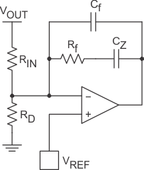 Figure 10. Voltage Amplifier Configuration
The gain of the voltage amplifier, GVA, is determined by first calculating the amount of ripple present on the output capacitor. The peak value of the second harmonic voltage is given by the equation:
In this example, VOPK is equal to 3.91 V. Assuming an allowable contribution of 0.75% (1.5% peak to peak) from the voltage loop to the total harmonic distortion budget, set the gain equal to:
where
- ΔVVAOUT is the effective output voltage range of the error amplifier (5 V for the UCC3817)
The network must realize this filter is comprised of an input resistor, RIN, and feedback components Cf, CZ, and Rf. The value of RIN is already determined, because of its function as one half of a resistor divider from VOUT feeding back to the voltage amplifier for output voltage regulation. In this case, the value was chosen to be 1 MΩ. This high value was chosen to reduce power dissipation in the resistor. In practice, the resistor value would be realized by the use of two 500-kΩ resistors in series, because of the voltage rating constraints of most standard 1/4-W resistors. The value of Cf is determined by the equation:
In this example, Cf equals 150 nF. Resistor Rf sets the dc gain of the error amplifier and thus determines the frequency of the pole of the error amplifier. The location of the pole can be found by setting the gain of the loop equation to one, and solving for the crossover frequency. The frequency, expressed in terms of input power, can be calculated by the equation:
fVI for this converter is 10 Hz. A derivation of this equation can be found in the Unitrode Power Supply Design Seminar SEM1000, Topic 1, [A 250-kHz, 500-W Power Factor Correction Circuit Employing Zero Voltage Transitions].
Solving for Rf becomes:
or Rf equals 100 kΩ.
Due to the low output impedance of the voltage amplifier, capacitor CZ was added in series with RF to reduce loading on the voltage divider. To ensure the voltage loop crossed over at fVI, CZ was selected to add a zero at a 10th of fVI. For the design in Figure 9, a 2.2-μF capacitor was chosen for CZ. The following equation can calculate CZ.

8.2.2.5 Current Loop
The gain of the power stage is:
RSENSE has been chosen to give the desired differential voltage for the current sense amplifier at the desired current limit point. In this example, a current limit of 4 A and a reasonable differential voltage to the current amp of 1 V gives a RSENSE value of 0.25 Ω. VP in this equation is the voltage swing of the oscillator ramp, 4 V for the UCC3817. Setting the crossover frequency of the system to 1/10th of the switching frequency, or 10 kHz, requires a power stage gain at that frequency of 0.383. For the system to have a gain of 1 at the crossover frequency, the current amplifier must have a gain of 1/GID at that frequency. GEA, the current amplifier gain is then:
RI is the RMOUT resistor, previously calculated to be 3.9 kΩ. (refer to Figure 11). The gain of the current amplifier is Rf/RI, so multiplying RI by GEA gives the value of Rf,which in this case is approximately 12 kΩ. Setting a zero at the crossover frequency and a pole at half the switching frequency completes the current loop compensation.
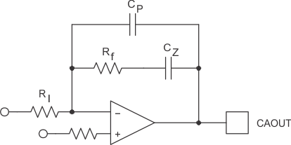 Figure 11. Current Loop Compensation
The UCC3817 current amplifier has the input from the multiplier applied to the inverting input. This change in architecture from previous Texas Instruments PFC controllers improves noise immunity in the current amplifier and adds a phase inversion into the control loop. The UCC3817 takes advantage of this phase inversion to implement leading-edge duty cycle modulation. Synchronizing a boost PFC controller to a downstream dc-to-dc controller reduces the ripple current seen by the bulk capacitor between stages, reducing capacitor size and cost and reducing EMI. This is explained in greater detail in Capacitor Ripple Reduction. The UCC3817 current amplifier configuration is shown in Figure 12.
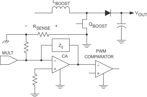 Figure 12. UCC3817 Current Amplifier Configuration
8.2.2.6 Start Up
The UCC3818 version of the device is intended to have VCC connected to a 12-V supply voltage. The UCC3817 has an internal shunt regulator, enabling the device to be powered from bootstrap circuitry as shown in Figure 9. The current drawn by the UCC3817 during undervoltage lockout, or start-up current, is typically 150 μA. Once VCC is above the UVLO threshold, the device is enabled and draws 4 mA typically. A resistor connected between the rectified ac line voltage and the VCC pin provides current to the shunt regulator during power up. Once the circuit is operational, the bootstrap winding of the inductor provides the VCC voltage. Sizing of the start-up resistor is determined by the start-up time requirement of the system design.
where
- IC is the charge current
- C is the total capacitance at the VCC pin
- ΔV is the UVLO threshold
- Δt is the allowed start-up time
Assuming a 1 second allowed start-up time, a 16-V VCC turn-on threshold, and a total VCC capacitance of 100 μF, a resistor value of 51 kΩ is required at a low line input voltage of 85 VRMS. The IC start-up current is sufficiently small as to be ignored in sizing the start-up resistor.
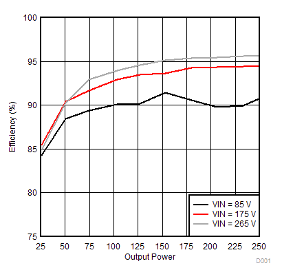
8.2.3 Application Curves
