SLUS157Q December 1999 – October 2019 UCC1895 , UCC2895 , UCC3895
PRODUCTION DATA.
- 1 Features
- 2 Applications
- 3 Description
- 4 Revision History
- 5 Pin Configuration and Functions
- 6 Specifications
-
7 Detailed Description
- 7.1 Overview
- 7.2 Functional Block Diagrams
- 7.3
Feature Description
- 7.3.1 ADS (Adaptive Delay Set)
- 7.3.2 CS (Current Sense)
- 7.3.3 CT (Oscillator Timing Capacitor)
- 7.3.4 DELAB and DELCD (Delay Programming Between Complementary Outputs)
- 7.3.5 EAOUT, EAP, and EAN (Error Amplifier)
- 7.3.6 OUTA, OUTB, OUTC, and OUTD (Output MOSFET Drivers)
- 7.3.7 PGND (Power Ground)
- 7.3.8 RAMP (Inverting Input of the PWM Comparator)
- 7.3.9 REF (Voltage Reference)
- 7.3.10 RT (Oscillator Timing Resistor)
- 7.3.11 GND (Analog Ground)
- 7.3.12 SS/DISB (Soft Start/Disable)
- 7.3.13 SYNC (Oscillator Synchronization)
- 7.3.14 VDD (Chip Supply)
- 7.4 Device Functional Modes
- 7.5 Programming
-
8 Application and Implementation
- 8.1 Application Information
- 8.2
Typical Application
- 8.2.1 Design Requirements
- 8.2.2
Detailed Design Procedure
- 8.2.2.1 Power Loss Budget
- 8.2.2.2 Preliminary Transformer Calculations (T1)
- 8.2.2.3 QA, QB, QC, QD FET Selection
- 8.2.2.4 Selecting LS
- 8.2.2.5 Selecting Diodes DB and DC
- 8.2.2.6 Output Inductor Selection (LOUT)
- 8.2.2.7 Output Capacitance (COUT)
- 8.2.2.8 Select Rectifier Diodes
- 8.2.2.9 Input Capacitance (CIN)
- 8.2.2.10 Current Sense Network (CT, RCS, RR, DA)
- 8.2.3 Application Curves
- 9 Power Supply Recommendations
- 10Layout
- 11Device and Documentation Support
- 12Mechanical, Packaging, and Orderable Information
Package Options
Mechanical Data (Package|Pins)
Thermal pad, mechanical data (Package|Pins)
- PW|20
Orderable Information
8.1 Application Information
A simplified electrical diagram of this converter is shown in Figure 18. The controller device is located on the primary side of converter to allow easy bias power generation.
The power stage includes primary side MOSFETs, QA, QB, QC and QD. Diode rectification is used here for simplicity but synchronous rectification is also possible and is described in application notes SLUU109Using the UCC3895 in a Direct Control Driven Synchronous Rectifier Applications and SLUA287Control Driven Synchronous Rectifiers In Phase Shifted Full Bridge Converters. The centre-tapped rectifier scheme with L-C output filter is a popular choice for the 12-V output converters in server power supplies.
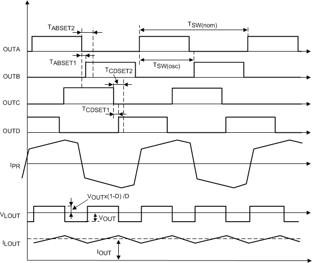
The major waveforms of the phase-shifted converter during normal operation are shown in Figure 17. The upper four waveforms show the output drive signals of the controller. Current, IPR, is the current flowing through the primary winding of the power transformer. The bottom two waveforms show the voltage at the output inductor, VLOUT, and the current through the output inductor, ILOUT. ZVS is an important feature for high input voltage converters in reducing switching losses associated with the internal parasitic capacitances of power switches and transformers. The controller ensures ZVS conditions over the entire load current range by adjusting the delay time between the primary MOSFETs switching in the same leg in accordance to the load variation. At light loads the output of the error amplifier (EAOUT) will drop below the threshold of the No-Load Comparator and the controller will enter a pulse skipping mode.
 Figure 17. Major Waveforms of Phase-Shifted Converter