SLLSER8I June 2017 – March 2024 UCC5310 , UCC5320 , UCC5350 , UCC5390
PRODUCTION DATA
- 1
- 1 Features
- 2 Applications
- 3 Description
- 4 Device Comparison Table
- 5 Pin Configuration and Function
-
6 Specifications
- 6.1 Absolute Maximum Ratings
- 6.2 ESD Ratings
- 6.3 Recommended Operating Conditions
- 6.4 Thermal Information
- 6.5 Power Ratings
- 6.6 Insulation Specifications for D Package
- 6.7 Insulation Specifications for DWV Package
- 6.8 Safety-Related Certifications For D Package
- 6.9 Safety-Related Certifications For DWV Package
- 6.10 Safety Limiting Values
- 6.11 Electrical Characteristics
- 6.12 Switching Characteristics
- 6.13 Insulation Characteristics Curves
- 6.14 Typical Characteristics
- 7 Parameter Measurement Information
- 8 Detailed Description
- 9 Application and Implementation
- 10Power Supply Recommendations
- 11Layout
- 12Device and Documentation Support
- 13Revision History
- 14Mechanical, Packaging, and Orderable Information
Package Options
Mechanical Data (Package|Pins)
Thermal pad, mechanical data (Package|Pins)
Orderable Information
8.3.4.1 Undervoltage Lockout (UVLO)
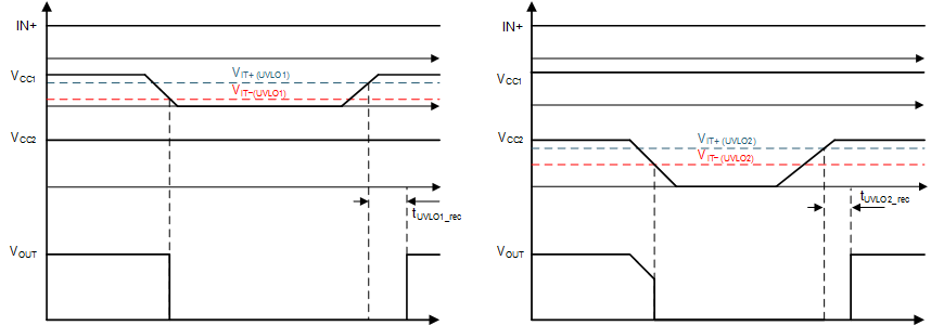
UVLO functions are implemented for both the VCC1 and VCC2 supplies between the VCC1 and GND1, and VCC2 and VEE2 pins to prevent an underdriven condition on IGBTs and MOSFETs. When VCC is lower than VIT+ (UVLO) at device start-up or lower than VIT–(UVLO) after start-up, the voltage-supply UVLO feature holds the effected output low, regardless of the input pins (IN+ and IN–) as shown in Table 8-2. The VCC UVLO protection has a hysteresis feature (Vhys(UVLO)). This hysteresis prevents chatter when the power supply produces ground noise; this allows the device to permit small drops in bias voltage, which occurs when the device starts switching and operating current consumption increases suddenly. Figure 8-9 shows the UVLO functions.
| CONDITION | INPUTS | OUTPUTS | ||
|---|---|---|---|---|
| IN+ | IN– | OUTH | OUT, OUTL | |
| VCC1 – GND1 < VIT+(UVLO1) during device start-up | H | L | Hi-Z | L |
| L | H | Hi-Z | L | |
| H | H | Hi-Z | L | |
| L | L | Hi-Z | L | |
| VCC1 – GND1 < VIT–(UVLO1) after device start-up | H | L | Hi-Z | L |
| L | H | Hi-Z | L | |
| H | H | Hi-Z | L | |
| L | L | Hi-Z | L | |
| CONDITION | INPUTS | OUTPUTS | ||
|---|---|---|---|---|
| IN+ | IN– | OUTH | OUT, OUTL | |
| VCC2 – VEE2 < VIT+(UVLO2) during device start-up | H | L | Hi-Z | L |
| L | H | Hi-Z | L | |
| H | H | Hi-Z | L | |
| L | L | Hi-Z | L | |
| VCC2 – VEE2 < VIT–(UVLO2) after device start-up | H | L | Hi-Z | L |
| L | H | Hi-Z | L | |
| H | H | Hi-Z | L | |
| L | L | Hi-Z | L | |
When VCC1 or VCC2 drops below the UVLO1 or UVLO2 threshold, a delay, tUVLO1_rec or tUVLO2_rec, occurs on the output when the supply voltage rises above VIT+(UVLO) or VIT+(UVLO2) again. Figure 8-9 shows this delay.
 Figure 8-9 UVLO Functions