SBOS913 February 2018 XTR305
PRODUCTION DATA.
- 1 Features
- 2 Applications
- 3 Description
- 4 Revision History
- 5 Pin Configuration and Functions
-
6 Specifications
- 6.1 Absolute Maximum Ratings
- 6.2 ESD Ratings
- 6.3 Recommended Operating Conditions
- 6.4 Thermal Information
- 6.5 Electrical Characteristics: Voltage Output Mode
- 6.6 Electrical Characteristics: Current Output Mode
- 6.7 Electrical Characteristics: Operational Amplifier (OPA)
- 6.8 Electrical Characteristics: Instrumentation Amplifier (IA)
- 6.9 Electrical Characteristics: Current Monitor
- 6.10 Electrical Characteristics: Power and Digital
- 6.11 Typical Characteristics
- 7 Detailed Description
-
8 Application and Implementation
- 8.1 Application Information
- 8.2
Typical Application
- 8.2.1 Design Requirements
- 8.2.2
Detailed Design Procedure
- 8.2.2.1 Voltage Output Mode
- 8.2.2.2 Current Output Mode
- 8.2.2.3 Input Signal Connection
- 8.2.2.4 Externally-Configured Mode: OPA and IA
- 8.2.2.5 Driver Output Disable
- 8.2.2.6 Driving Capacitive Loads and Loop Compensation
- 8.2.2.7 Internal Current Sources, Switching Noise, and Settling Time
- 8.2.2.8 IA Structure, Voltage Monitor
- 8.2.2.9 Digital I/O and Ground Considerations
- 8.2.2.10 Output Protection
- 8.2.3 Application Curves
- 9 Power Supply Recommendations
- 10Layout
- 11Device and Documentation Support
- 12Mechanical, Packaging, and Orderable Information
Package Options
Mechanical Data (Package|Pins)
- RGW|20
Thermal pad, mechanical data (Package|Pins)
- RGW|20
Orderable Information
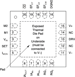
5 Pin Configuration and Functions
RGW Package
20-Pin VQFN With Thermal Pad
Top View

Pin Functions
| PIN | I/O | DESCRIPTION | |
|---|---|---|---|
| NO. | NAME | ||
| 1 | M2 | I | Mode input |
| 2 | M1 | I | Mode input |
| 3 | VIN | I | Noninverting signal input |
| 4 | SET | I | Input for gain setting; inverting input |
| 5 | IMON | O | Current monitor output |
| 6 | IAOUT | O | Instrumentation amplifier signal output |
| 7 | IAIN– | I | Instrumentation amplifier inverting input |
| 8 | IAIN+ | I | Instrumentation amplifier noninverting input |
| 9 | RG1 | I | Instrumentation amplifier gain resistor |
| 10 | RG2 | I | Instrumentation amplifier gain resistor |
| 11 | V– | - | Negative power supply |
| 12 | NC | - | No internal connection |
| 13 | DRV | O | Operational amplifier output |
| 14 | NC | - | No internal connection |
| 15 | V+ | - | Positive power supply |
| 16 | DGND | - | Ground for digital I/O |
| 17 | EFCM | O | Error flag for common mode over range, active low |
| 18 | EFLD | O | Error flag for load error, active low |
| 19 | EFOT | O | Error flag for over temperature, active low |
| 20 | OD | I | Output disable, disabled low |
| Pad | Exposed Pad | - | Exposed thermal pad must be connected to V− |