SBAS490B December 2011 – May 2015 DAC1282
PRODUCTION DATA.
- 1 Features
- 2 Applications
- 3 Description
- 4 Revision History
- 5 Device Comparison
- 6 Pin Configuration and Functions
- 7 Specifications
-
8 Detailed Description
- 8.1 Overview
- 8.2
Feature Description
- 8.2.1 Signal Output (VOUTP, VOUTN)
- 8.2.2 DAC Modes
- 8.2.3 Reference Voltage (VREF)
- 8.2.4 Output Filter (CAPP, CAPN)
- 8.2.5 Output Switch (SWINP, SWINN, SWOUTP, SWOUTN)
- 8.2.6 Clock Input (CLK)
- 8.2.7 Switch Control/External Digital Input (SW/TD)
- 8.2.8 SYNC
- 8.2.9 RESET/PWDN
- 8.2.10 AVDD, AVSS, and DVDD Power Supplies
- 8.2.11 Step Response
- 8.2.12 Frequency Response
- 8.3 Device Functional Modes
- 8.4 Programming
- 8.5 Register Map
- 9 Application and Implementation
- 10Device and Documentation Support
- 11Mechanical, Packaging, and Orderable Information
Package Options
Mechanical Data (Package|Pins)
- PW|24
Thermal pad, mechanical data (Package|Pins)
Orderable Information
1 Features
- Single-Chip Test Signal Generator
- Buffered Voltage Output
- High Performance:
- THD: –125 dB (G = 1/1 to 1/8)
- SNR: 120 dB (413 Hz BW, G = 1/1)
- Analog and Digital Gain Control
- Output Frequency: 0.488 Hz to 250 Hz
- Sine, Pulse, and DC Modes
- Digital Data Input Mode
- Low On-Resistance Signal Switch
- Sync Input
- Power-Down Mode
- Analog Supply: 5 V or ±2.5 V
- Digital Supply: 1.8 V to 3.3 V
- Power: 38 mW
- Package: TSSOP-24
- Operating Range: –50°C to +125°C
2 Applications
- Energy Exploration
- Seismic Monitoring Systems
- High-Accuracy Instrumentation
3 Description
The DAC1282 is a fully-integrated digital-to-analog converter (DAC) providing low distortion, digital synthesized voltage output suitable for testing of seismic equipment. The DAC1282 achieves very high performance in a small package with low power. Together, with the high-performance ADS1281 and ADS1282 analog-to-digital converters (ADCs), these devices create a measurement system that meets the exacting demands of seismic data acquisition equipment.
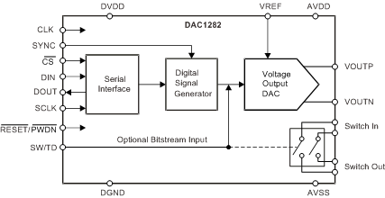
The DAC1282 integrates a digital signal generator, a DAC, and an output amplifier providing sine wave, dc, and pulse output voltages.
The output frequency is programmable from 0.5 Hz to 250 Hz and the magnitude is scaled by both analog and digital control. The analog gain is adjustable in 6-dB steps and the digital gain in 0.5-dB steps. The analog gain settings match those of the ADS1282 for testing at all gains with high resolution.
The DAC1282 also provides pulse outputs. The pulse amplitude is user-programmed and then selected by the pin for precise timing. Custom output signals can be generated by applying an external bitstream pattern.
A signal switch can be used to connect the DAC output to sensors for THD and impulse testing. The switch timing is controlled by pin and by command.
A SYNC pin synchronizes the DAC output to the analog-to-digital converter (ADC) sample interval. A power-down input disables the device, reducing power consumption to microwatts.

4 Revision History
Changes from A Revision (September 2012) to B Revision
- Added ADS1282A device to data sheetGo
Changes from * Revision (December 2011) to A Revision