JAJSQH3C september   2009  – june 2023 ADS1000-Q1

PRODUCTION DATA  

  1.   1
  2. 特長
  3. アプリケーション
  4. 概要
  5. Revision History
  6. Pin Configuration and Functions
  7. Specifications
    1. 6.1 Absolute Maximum Ratings
    2. 6.2 ESD Ratings
    3. 6.3 Recommended Operating Conditions
    4. 6.4 Thermal Information
    5. 6.5 Electrical Characteristics
    6. 6.6 Timing Requirements
    7. 6.7 Timing Diagram
    8. 6.8 Typical Characteristics
  8. Detailed Description
    1. 7.1 Overview
    2. 7.2 Functional Block Diagram
    3. 7.3 Feature Description
      1. 7.3.1 Analog-to-Digital Converter
      2. 7.3.2 Clock Generator
    4. 7.4 Device Functional Modes
      1. 7.4.1 Operating Modes
      2. 7.4.2 Reset and Power Up
    5. 7.5 Programming
      1. 7.5.1 I2C Interface
      2. 7.5.2 ADS1000-Q1 I2C Addresses
      3. 7.5.3 I2C General Call
      4. 7.5.4 I2C Data Rates
      5. 7.5.5 Output Code Calculation
    6. 7.6 Register Maps
      1. 7.6.1 Output Register
      2. 7.6.2 Configuration Register
      3. 7.6.3 Reading From the ADS1000-Q1
      4. 7.6.4 Writing to the ADS1000-Q1
  9. Application and Implementation
    1. 8.1 Application Information
      1. 8.1.1 Basic Connections
        1. 8.1.1.1 Connecting Multiple Devices
        2. 8.1.1.2 Using GPIO Ports For I2C
        3. 8.1.1.3 Single-Ended Inputs
    2. 8.2 Typical Applications
      1. 8.2.1 ADS1000-Q1 With Current-Shunt Monitor
        1. 8.2.1.1 Design Requirements
        2. 8.2.1.2 Detailed Design Procedure
          1. 8.2.1.2.1 Part Selection
            1. 8.2.1.2.1.1 Gain Settings
            2. 8.2.1.2.1.2 Circuit Implementation
        3. 8.2.1.3 Application Curve
      2. 8.2.2 Low-Side Current Measurement
        1. 8.2.2.1 Design Requirements
        2. 8.2.2.2 Detailed Design Procedure
    3. 8.3 Power Supply Recommendations
    4. 8.4 Layout
      1. 8.4.1 Layout Guidelines
      2. 8.4.2 Layout Example
  10. Device and Documentation Support
    1. 9.1 ドキュメントの更新通知を受け取る方法
    2. 9.2 サポート・リソース
    3. 9.3 Trademarks
    4. 9.4 静電気放電に関する注意事項
    5. 9.5 用語集
  11. 10Mechanical, Packaging, and Orderable Information

パッケージ・オプション

メカニカル・データ(パッケージ|ピン)
サーマルパッド・メカニカル・データ
発注情報

Single-Ended Inputs

Although the ADS1000-Q1 has a fully differential input, the device can easily measure single-ended signals. A simple single-ended connection scheme is shown in Figure 8-4. The ADS1000-Q1 is configured for single-ended measurement by grounding either of the input pins, usually VIN–, and applying the input signal to VIN+. The single-ended signal can range from –0.2 V to AVDD + 0.2 V. The ADS1000-Q1 loses no linearity anywhere in the input range. Negative voltages cannot be applied to this circuit because the ADS1000-Q1 inputs can only accept positive voltages.
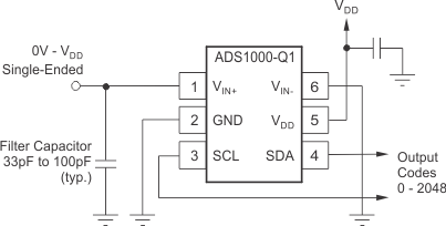
GUID-C69735D2-589F-4518-8BB6-191AA5C32065-low.gif Figure 8-4 Measuring Single-Ended Inputs

The ADS1000-Q1 input range is bipolar differential with respect to the reference, that is, ±VDD. The single-ended circuit shown in Figure 8-4 covers only half the ADS1000-Q1 input scale because this circuit does not produce differentially negative inputs; therefore, one bit of resolution is lost.