JAJSPW8E march 2011 – february 2023 ADS4222 , ADS4225 , ADS4226 , ADS4242 , ADS4245 , ADS4246
PRODUCTION DATA
- 1 特長
- 2 アプリケーション
- 3 概要
- 4 Revision History
- 5 概要 (続き)
- 6 Pin Configuration and Functions
-
7 Specifications
- 7.1 Absolute Maximum Ratings
- 7.2 ESD Ratings
- 7.3 Recommended Operating Conditions
- 7.4 Thermal Information
- 7.5 Electrical Characteristics: ADS4246, ADS4245, ADS4242
- 7.6 Electrical Characteristics: ADS4226, ADS4225, ADS4222
- 7.7 Electrical Characteristics: General
- 7.8 Digital Characteristics
- 7.9 Timing Requirements: LVDS and CMOS Modes #GUID-C6C0701B-A11B-492F-BD6B-B774F5FE4665/SLAS6895399
- 7.10 Serial Interface Timing Characteristics #GUID-3852E7CE-C5B6-42F5-A56A-70AB1B981302/SBAS5097810
- 7.11 Reset Timing (Only When Serial Interface Is Used)
- 7.12 Typical Characteristics
-
8 Detailed Description
- 8.1 Overview
- 8.2 Functional Block Diagrams
- 8.3 Feature Description
- 8.4 Device Functional Modes
- 8.5 Programming
- 8.6 Register Maps
- 9 Application and Implementation
- 10Device and Documentation Support
- 11Mechanical, Packaging, and Orderable Information
パッケージ・オプション
メカニカル・データ(パッケージ|ピン)
- RGC|64
サーマルパッド・メカニカル・データ
- RGC|64
発注情報
8.5.5 Parallel Configuration Details
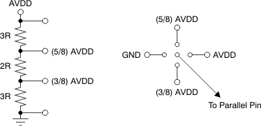
The functions controlled by each parallel pin are described in Table 8-6, Table 8-7, and Table 8-8. A simple way of configuring the parallel pins is shown in Figure 8-16.
Table 8-6 SCLK Control Pin
| VOLTAGE APPLIED ON SCLK | DESCRIPTION |
|---|---|
| Low | Low-speed mode is disabled |
| High | Low-speed mode is enabled(1) |
(1) Low-speed mode is enabled in the ADS4222/42 by default.
Table 8-7 SEN Control Pin
| VOLTAGE APPLIED ON SEN | DESCRIPTION |
|---|---|
| 0 (+50 mV/0 mV) | Twos complement and parallel CMOS output |
| (3/8) AVDD (±50 mV) | Offset binary and parallel CMOS output |
| (5/8) 2AVDD (±50 mV) | Offset binary and DDR LVDS output |
| AVDD (0 mV/–50 mV) | Twos complement and DDR LVDS output |
Table 8-8 CTRL1, CTRL2, and CTRL3 Pins
| CTRL1 | CTRL2 | CTRL3 | DESCRIPTION |
|---|---|---|---|
| Low | Low | Low | Normal operation |
| Low | Low | High | Not available |
| Low | High | Low | Not available |
| Low | High | High | Not available |
| High | Low | Low | Global power-down |
| High | Low | High | Channel A standby, channel B is active |
| High | High | Low | Not available |
| High | High | High | MUX mode of operation, channel A and B data are multiplexed and output on the DB[13:0] pins. |
 Figure 8-16 Simple Scheme to Configure the Parallel Pins