JAJSO07B December 2012 – April 2022 ADS54T01
PRODUCTION DATA
- 1 特長
- 2 アプリケーション
- 3 概要
- 4 Revision History
- 5 Device Comparison
- 6 Pin Configuration and Functions
- 7 Specifications
-
8 Detailed Description
- 8.1 Overview
- 8.2 Functional Block Diagram
- 8.3
Feature Description
- 8.3.1 Test Pattern Output
- 8.3.2 Clock Inputs
- 8.3.3 SNR and Clock Jitter
- 8.3.4 Analog Inputs
- 8.3.5 Over-Range Indication
- 8.3.6 Interleaving Correction
- 8.3.7 High-Resolution Output Data
- 8.3.8 Low-Resolution Output Data
- 8.3.9 Full Speed – 7 Bit
- 8.3.10 Decimated Low-Resolution Output Data
- 8.3.11 Multi Device Synchronization
- 8.4 Device Functional Modes
- 8.5 Programming
- 8.6 Register Maps
- 9 Power Supply Recommendations
- 10Device and Documentation Support
- 11Mechanical, Packaging, and Orderable Information
8.3.1 Test Pattern Output
The ADS54T01 can be configured to output different test patterns that can be used to verify the digital interface is connected and working properly.
To enable the test pattern mode, the high-performance mode 1 has to be disabled first through the SPI register write. Then different test patterns can be selected by configuring registers x3C, x3D, and x3E. All three registers must be configured for the test pattern to work properly.
First set HP1 = 0 (Addr 0x01, D01)
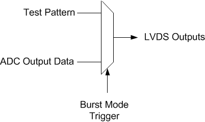
Internally the test pattern replaces the sampled data from the ADC. However at the LVDS outputs the output data is still subject to burst mode operation. In low-resolution output, the LSBs of the test pattern are replaced with 0 s.
 Figure 8-2 Test Pattern Selection
| Register Address | All 0s | All 1s | Toggle (0xAAA => 0x555) | Toggle (0xFFF => 0x000) |
|---|---|---|---|---|
| 0x3C | 0x8000 | 0xBFFC | 0x9554 | 0xBFFC |
| 0x3D | 0x0000 | 0x3FFC | 0x2AA8 | 0x0000 |
| 0x3E | 0x0000 | 0x3FFC | 0x1554 | 0x3FFC |
| Register Address | Custom Pattern | |||||||||||||||
|---|---|---|---|---|---|---|---|---|---|---|---|---|---|---|---|---|
| D15 | D14 | D13 | D12 | D11 | D10 | D9 | D8 | D7 | D6 | D5 | D4 | D3 | D2 | D1 | D0 | |
| x3C | 1 | 0 | D11 | D10 | D9 | D8 | D7 | D6 | D5 | D4 | D3 | D2 | D1 | D0 | 0 | 0 |
| x3D | 0 | 0 | 0 | 0 | ||||||||||||
| x3E | 0 | 0 | 0 | 0 | ||||||||||||
For normal operation, set HP1 = 1 (Addr 0x01, D01) and 0x3C, 0x3D, and 0x3E all to 0.