SLOS729D October 2011 – November 2015 AFE5808A
PRODUCTION DATA.
- 1 Features
- 2 Applications
- 3 Description
- 4 Revision History
- 5 Description (continued)
- 6 Pin Configuration and Functions
- 7 Specifications
-
8 Detailed Description
- 8.1 Overview
- 8.2 Functional Block Diagram
- 8.3 Feature Description
- 8.4 Device Functional Modes
- 8.5 Programming
- 8.6
Register Maps
- 8.6.1 ADC Register Map
- 8.6.2
ADC Register/Digital Processing Description
- 8.6.2.1 AVERAGING_ENABLE: Address: 2[11]
- 8.6.2.2 ADC_OUTPUT_FORMAT: Address: 4[3]
- 8.6.2.3 DIGITAL_GAIN_ENABLE: Address: 3[12]
- 8.6.2.4 DIGITAL_HPF_ENABLE
- 8.6.2.5 DIGITAL_HPF_FILTER_K_CHX
- 8.6.2.6 LOW_FREQUENCY_NOISE_SUPPRESSION: Address: 1[11]
- 8.6.2.7 LVDS_OUTPUT_RATE_2X: Address: 1[14]
- 8.6.2.8 CHANNEL_OFFSET_SUBSTRACTION_ENABLE: Address: 3[8]
- 8.6.2.9 SERIALIZED_DATA_RATE: Address: 3[14:13]
- 8.6.2.10 TEST_PATTERN_MODES: Address: 2[15:13]
- 8.6.2.11 SYNC_PATTERN: Address: 10[8]
- 8.6.3 VCA Register Map
- 8.6.4 AFE5808A VCA Register Description
-
9 Application and Implementation
- 9.1 Application Information
- 9.2 Typical Application
- 9.3
Do's and Don'ts
- 9.3.1 Driving the Inputs (Analog or Digital) Beyond the Power-Supply Rails
- 9.3.2 Driving the Device Signal Input With an Excessively High Level Signal
- 9.3.3 Driving the VCNTL Signal With an Excessive Noise Source
- 9.3.4 Using a Clock Source With Excessive Jitter, an Excessively Long Input Clock Signal Trace, or Having Other Signals Coupled to the ADC or CW Clock Signal Trace
- 9.3.5 LVDS Routing Length Mismatch
- 9.3.6 Failure to Provide Adequate Heat Removal
- 10Power Supply Recommendations
- 11Layout
- 12Device and Documentation Support
- 13Mechanical, Packaging, and Orderable Information
9 Application and Implementation
NOTE
Information in the following applications sections is not part of the TI component specification, and TI does not warrant its accuracy or completeness. TI’s customers are responsible for determining suitability of components for their purposes. Customers should validate and test their design implementation to confirm system functionality.
9.1 Application Information
The AFE5808A device is a highly integrated analog front-end solution. To maximize its performance, users must carefully optimize its surrounding circuits, such as T/R switch, VCNTL circuits, audio ADCs for CW path, clock distribution network, synchronized power supplies and digital processors. Some common practices are described below.
Table 13 lists companion TI devices that are used to complete the analog signal chain in a system.
Table 13. Application Companion Devices
| PART NUMBER | PART DESCRIPTION | FUNCTIONS |
|---|---|---|
| THS4130, SLOS318 | Fully Differential Input/Output Low Noise Amplifier With Shutdown | TGC VCNTL Opamp, CW summing amplifier and active filter |
| OPA1632, SBOS286 | Fully Differential I/O Audio Amplifier | TGC VCNTL amplifier, CW summing amplifier and active filter |
| OPA2211, SBOS377 | 1.1nV/√Hz Noise, Low Power, Precision Operational Amplifier | CW summing amplifier and active filter |
| LME49990, SNOSB16 | Ultra-low Distortion, Ultra-low Noise Operational Amplifier | CW summing amplifier and active filter |
| LMH6629, SNOSB18 | Ultra-Low Noise, High-Speed Operational Amplifier with Shutdown | CW summing amplifier and active filter |
| ADS8413, SLAS490 | 16-bit, Unipolar Diff Input, 2MSPS Sampling rate, 4.75V to 5.25V ADC with LVDS Serial Interface | CW Audio ADC |
| ADS8881, SBAS547 | 18-Bit, 1-MSPS, Serial Interface, microPower, Truly-Differential Input, SAR ADC | CW Audio ADC |
| DAC7811, SBAS337 | 12-Bit, Serial Input, Multiplying Digital to Analog Converter | TGC VCNTL Digital to Analog Converter |
| LMK04800, SNAS489 | Low Noise Clock Jitter Cleaner With Dual Cascaded PLLs and Integrated 1.9 GHz VCO | Jitter cleaner and clock synthesizer |
| CDCM7005, SCAS793 | High Performance, Low Phase Noise, Low Skew Clock Synchronizer | Jitter cleaner and clock synthesizer |
| CDCE72010, SCAS858 | 10 Outputs Low Jitter Clock Synchronizer and Jitter Cleaner | Jitter cleaner and clock synthesizer |
| CDCLVP1208, SCAS890 | Low Jitter, 2-Input Selectable 1:8 Universal-to-LVPECL Buffer | Clock buffer |
| LMK00308, SNAS576 | 3.1-GHz Differential Clock Buffer/Level Translator | Clock buffer |
| LMK01000, SNAS437 | 1.6 GHz High Performance Clock Buffer, Divider, and Distributor | Clock buffer |
| SN74AUP1T04, SCES800 | Low Power, 1.8/2.5/3.3-V Input, 3.3-V CMOS Output, Single Inverter Gate | 1.8V/2.5V/3.3V Level shifter for SPI |
| UCC28250, SLUSA29 | Advanced PWM Controller with Pre-Bias Operation | Synchronized DC-DC power supply controller |
9.2 Typical Application
Figure 80 lists a typical application circuit diagram. The configuration for each block is discussed in the following sections.
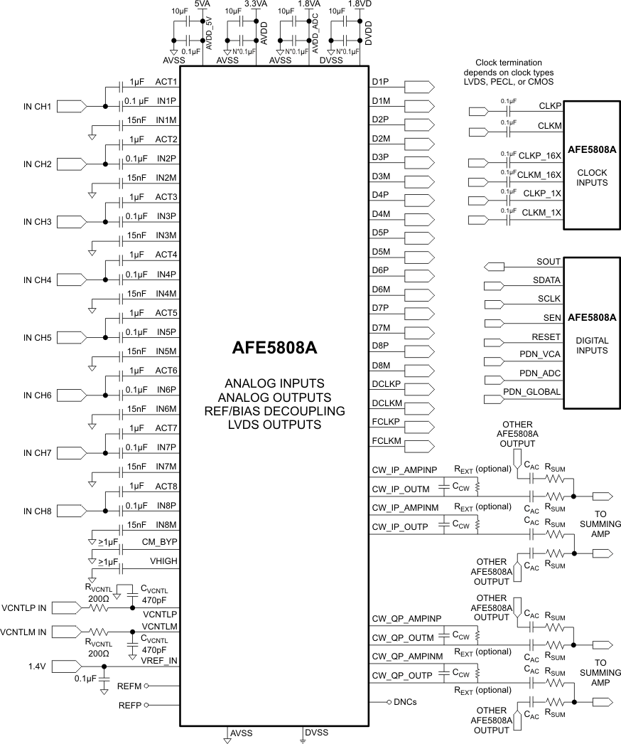 Figure 80. Typical Application Circuit
9.2.1 Design Requirements
Table 14 shows the typical requirements for a traditional medical ultrasound imaging system.
Table 14. Design Parameters
| PARAMETER | EXAMPLE VALUES |
|---|---|
| Signal center frequency (f0) | 1 MHz to approximately 20 MHz |
| Signal bandwidth (BW) | 10% to approximately 100% of f0 |
| Overloaded signals due to T/R switch leakage | approximately 2 VPP |
| Maximum input signal amplitude | 100 mVPP to 1 VPP |
| Transducer noise level | 1 nV/√Hz |
| Dynamic range | 151 dBc/Hz |
| Time gain compensation range | 40 dB |
| Total harmonic distortion | 40 dBc at 5MHz |
9.2.2 Detailed Design Procedure
Medical ultrasound imaging is a widely-used diagnostic technique that enables visualization of internal organs including their size, structure, and blood flow estimation. An ultrasound system uses a focal imaging technique that involves time shifting, scaling, and intelligently summing the echo energy using an array of transducers to achieve high imaging performance. The concept of focal imaging provides the ability to focus on a single point in the scan region. By subsequently focusing at different points, an image is assembled.
When initiating an imaging, a pulse is generated and transmitted from each of the 64 transducer elements. The pulse, now in the form of mechanical energy, propagates through the body as sound waves, typically in the frequency range of 1 MHz to 15 MHz. The sound waves are attenuated as they travel through the objects being imaged, and the attenuation coefficients ɑ are about 0.54 dB/(MHz×cm) in soft tissue and 6 to approximately 10 dB/(MHz×cm) in bone. Most medical ultrasound systems use the reflection imaging mode and the total signal attenuation is calculated by 2 × depth × ɑ × f0. As the signal travels, portions of the wave front energy are reflected. Signals that are reflected immediately after transmission are very strong because they are from reflections close to the surface; reflections that occur long after the transmit pulse are very weak because they are reflecting from deep in the body. As a result of the limitations on the amount of energy that can be put into the imaging object, the industry developed extremely sensitive receive electronics with wide dynamic range.
Receive echoes from focal points close to the surface require little, if any, amplification. This region is referred to as the near field. However, receive echoes from focal points deep in the body are extremely weak and must be amplified by a factor of 100 or more. This region is referred to as the far field. In the high-gain (far field) mode, the limit of performance is the sum of all noise sources in the receive chain. In high-gain (far field) mode, system performance is defined by its overall noise level, which is limited by the noise level of the transducer assembly and the receive low-noise amplifier (LNA). However in the low-gain (near field) mode, system performance is defined by the maximum amplitude of the input signal that the system can handle. The ratio between noise levels in high-gain mode and the signal amplitude level in low-gain mode is defined as the dynamic range of the system. The high integration and high dynamic range of the device make it ideally suited for ultrasound imaging applications.
The device includes an integrated LNA and VCAT (which use the gain that can be changed with enough time to handle both near- and far-field systems), a low-pass antialiasing filter to limit the noise bandwidth, an ADC with high SNR performance, and a CW mixer. Figure 80 illustrates an application circuit of the device.
Use the following steps to design medical ultrasound imaging systems:
1. Use the signal center frequency and signal bandwidth to select an appropriate ADC sampling frequency.
2. Use the time gain compensation range to select the range of the VCNTL signal.
3. Use the transducer noise level and maximum input signal amplitude to select the appropriate LNA gain. The device input-referred noise level reduces with higher LNA gain. However, higher LNA gain leads to lower input signal swing support.
4. Select different passive components for different device pins as shown in Figure 80.
5. Select the appropriate input termination configuration as discussed in Active Termination.
6. Select the clock configuration for the ADC and CW clocks as discussed in CW Clock Selection and ADC Clock Configurations.
9.2.2.1 LNA Configuration
9.2.2.1.1 LNA Input Coupling and Decoupling
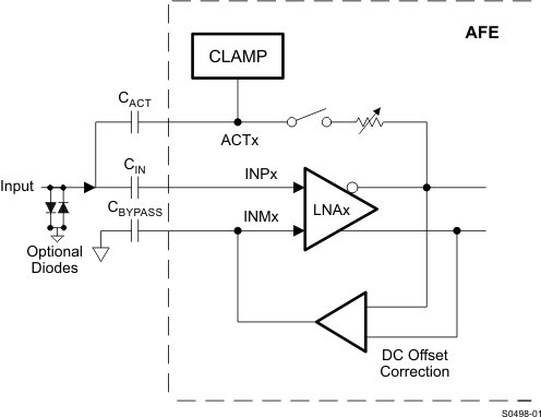
The LNA closed-loop architecture is internally compensated for maximum stability without the need of external compensation components. The LNA inputs are biased at 2.4 V and AC coupling is required. A typical input configuration is shown in Figure 81. CIN is the input AC coupling capacitor. CACT is a part of the active termination feedback path. Even if the active termination is not used, the CACT is required for the clamp functionality. Recommended values for CACT = 1 µF and CIN are ≥ 0.1 µF. A pair of clamping diodes is commonly placed between the T/R switch and the LNA input. Schottky diodes with suitable forward drop voltage (for example, the BAT754/54 series, the BAS40 series, the MMBD7000 series, or similar) can be considered depending on the transducer echo amplitude.
This architecture minimizes any loading of the signal source that may otherwise lead to a frequency-dependent voltage divider. The closed-loop design yields low offsets and offset drift. CBYPASS (≥0.015 µF) is used to set the high-pass filter cut-off frequency and decouple the complimentary input. Its cut-off frequency is inversely proportional to the CBYPASS value, The HPF cut-off frequency can be adjusted through the register 59[3:2] a Table 15 lists. Low frequency signals at T/R switch output, such as signals with slow ringing, can be filtered out. In addition, the HPF can minimize system noise from DC-DC converters, pulse repetition frequency (PRF) trigger, and frame clock. Most ultrasound systems’ signal processing unit includes digital high-pass filters or band-pass filters (BPFs) in FPGAs or ASICs. Further noise suppression can be achieved in these blocks. In addition, a digital HPF is available in the AFE5808A ADC. If low frequency signal detection is desired in some applications, the LNA HPF can be disabled.
Table 15. LNA HPF Settings (CBYPASS = 15 nF)
| Reg59[3:2] (0x3B[3:2]) | FREQUENCY |
|---|---|
| 00 | 100 kHz |
| 01 | 50 kHz |
| 10 | 200 kHz |
| 11 | 150 kHz |
CM_BYP and VHIGH pins, which generate internal reference voltages, need to be decoupled with ≥ 1-µF capacitors. Bigger bypassing capacitors (> 2.2 µF) may be beneficial if low frequency noise exists in system.
9.2.2.1.2 LNA Noise Contribution
The noise spec is critical for LNA and it determines the dynamic range of entire system. The LNA of the AFE5808A achieves low power and an exceptionally low-noise voltage of 0.63 nV/√Hz, and a low current noise of 2.7 pA/√Hz.
Typical ultrasonic transducer’s impedance Rs varies from tens of ohms to several hundreds of ohms. Voltage noise is the dominant noise in most cases; however, the LNA current noise flowing through the source impedance (Rs) generates additional voltage noise.

The AFE5808A device achieves low noise figure (NF) over a wide range of source resistances as shown in Figure 32, Figure 33, and Figure 34.
9.2.2.1.3 Active Termination
In ultrasound applications, signal reflection exists due to long cables between transducer and system. The reflection results in extra ringing added to echo signals in PW mode. Since the axial resolution depends on echo signal length, such ringing effect can degrade the axial resolution. Hence, either passive termination or active termination, is preferred if good axial resolution is desired. Figure 82 shows three termination configurations:
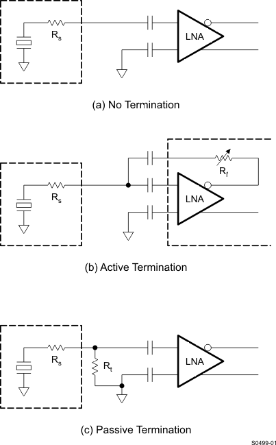 Figure 82. Termination Configurations
Under the no termination configuration, the input impedance of the AFE5808A device is about 6 kΩ (8 K//20 pF) at 1 MHz. Passive termination requires external termination resistor Rt, which contributes to additional thermal noise.
The LNA supports active termination with programmable values, as shown in Figure 83.
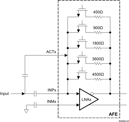 Figure 83. Active Termination Implementation
The AFE5808A device has four pre-settings 50 Ω,100 Ω, 200 Ω, and 400 Ω, which are configurable through the registers. Other termination values can be realized by setting the termination switches shown in Figure 83. Register [52] is used to enable these switches. The input impedance of the LNA under the active termination configuration approximately follows:

Table 7 lists the LNA RINs under different LNA gains. System designers can achieve fine tuning for different probes.
The equivalent input impedance is given by Equation 7, where RIN (8 K) and CIN (20 pF) are the input resistance and capacitance of the LNA.

Therefore the ZIN is frequency dependent and it decreases as frequency increases shown in Figure 10. Since approximately 2 MHz to 10 MHz is the most commonly used frequency range in medical ultrasound, this rolling-off effect does not impact system performance greatly. Active termination can be applied to both CW and TGC modes. Because each ultrasound system includes multiple transducers with different impedances, the flexibility of impedance configuration is a great plus.
Figure 32, Figure 33, and Figure 34 shows the NF under different termination configurations. It indicates that no termination achieves the best noise figure; active termination adds less noise than passive termination. Thus termination topology should be carefully selected based on each use scenario in ultrasound.
9.2.2.1.4 LNA Gain Switch Response
The LNA gain is programmable through SPI. The gain switching time depends on the SPI speed as well as the LNA gain response time. During the switching, glitches might occur and they can appear as artifacts in images. LNA gain switching in a single imaging line may not be preferred, although digital signal processing might be used here for glitch suppression.
9.2.2.2 Voltage-Controlled-Attenuator
The attenuator in the AFE5808A device is controlled by a pair of differential control inputs, the VCNTLM/P pins. The differential control voltage spans from 0 V to 1.5 V. This control voltage varies the attenuation of the attenuator based on its linear-in-dB characteristic. AFE5808A's maximum attenuation (minimum channel gain) appears at VCNTLP – VCNTLM= 1.5 V, and minimum attenuation (maximum channel gain) occurs at VCNTLP – VCNTLM = 0. The typical gain range is 40 dB and remains constant, independent of the PGA setting.
When only single-ended VCNTL signal is available, this 1.5-VPP signal can be applied on the VCNTLP pin with the VCNTLM pin connected to ground. As shown in Figure 84, TGC gain curve is inversely proportional to the VCNTLP – VCNTLM.
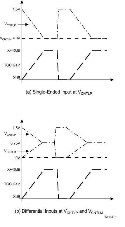 Figure 84. VCNTLP and VCNTLM Configurations
As discussed in the theory of operation, the attenuator architecture uses seven attenuator segments that are equally spaced in order to approximate the linear-in-dB gain-control slope. This approximation results in a monotonic slope; the gain ripple is typically less than ±0.5 dB.
The control voltage input (VCNTLM/P pins) represents a high-impedance input. The VCNTLM/P pins of multiple AFE5808A devices can be connected in parallel with no significant loading effects. When the voltage level (VCNTLP-VCNTLM) is above 1.5 V or below 0 V, the attenuator continues to operate at its maximum attenuation level or minimum attenuation level respectively. TI recommends limiting the voltage from –0.3 V to 2 V.
When the AFE5808A device operates in CW mode, the attenuator stage remains connected to the LNA outputs. Therefore, TI recommends powering down the VCA using the PDN_VCA register bit. In this case, VCNTLP – VCNTLM voltage does not matter.
The AFE5808A gain-control input has a –3-dB bandwidth of approximately 800 kHz. This wide bandwidth, although useful in many applications (for example fast VCNTL response), can also allow high-frequency noise to modulate the gain control input and finally affect the Doppler performance. In practice, this modulation can easily be avoided by additional external filtering (RVCNTL and CVCNTL) at VCNTLM/P pins as Figure 75 shows. However, the external filter's cut-off frequency cannot be kept too low as this results in low gain response time. Without external filtering, the gain control response time is typically less than 1 μs to settle within 10% of the final signal level of 1 VPP (–6 dBFS) output as indicated in Figure 51 and Figure 52.
Typical VCNTLM/P signals are generated by an 8 to 12 bit 10 MSPS digital to analog converter (DAC) and a differential operation amplifier. TI’s DACs, such as TLV5626 and DAC7821/11 (10 MSPS/ 12 bit), could be used to generate TGC control waveforms. Differential amplifiers with output common mode voltage control (for example THS4130 and OPA1632) can connect the DAC to the VCNTLM/P pins. The buffer amplifier can also be configured as an active filter to suppress low frequency noise. The VCNTLM/P circuit shall achieve low noise in order to prevent the VCNTLM/P noise being modulated to RF signals. TI recommends that VCNTLM/P noise is below 25 nV/√Hz at 1 kHz and 5 nV/√Hz at 50 kHz.In high channel count premium systems, the VCNTLM/P noise requirement is higher as shown in Figure 85.
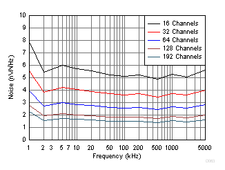 Figure 85. Allowed Noise on the VCNTL Signal Across Frequency and Different Channels
More information can be found in the data sheet, THS413x High-Speed, Low-Noise, Fully-Differential I/O Amplifiers (SLOS318), and the application note, Design for a Wideband Differential Transimpedance DAC Output (SBAA150). The VCNTL vs Gain curves can be found in Figure 2. Table 16 shows the absolute gain vs VCNTL, which may help program DAC correspondingly.
In PW Doppler and color Doppler modes, VCNTL noise should be minimized to achieve the best close-in phase noise and SNR. Digital VCNTL feature is implemented to address this need in the AFE5808A device. In the digital VCNTL mode, no external VCNTL is needed.
Table 16. VCNTLP–VCNTLM vs Gain Under Different LNA and PGA Gain Settings (Low Noise Mode)
| VCNTLP – VCNTLM
(V) |
Gain (dB) LNA = 12 dB PGA = 24 dB |
Gain (dB) LNA = 18 dB PGA = 24 dB |
Gain (dB) LNA = 24 dB PGA = 24 dB |
Gain (dB) LNA = 12 dB PGA = 30 dB |
Gain (dB) LNA = 18 dB PGA = 30 dB |
Gain (dB) LNA = 24 dB PGA = 30 dB |
|---|---|---|---|---|---|---|
| 0 | 36.45 | 42.45 | 48.45 | 42.25 | 48.25 | 54.25 |
| 0.1 | 33.91 | 39.91 | 45.91 | 39.71 | 45.71 | 51.71 |
| 0.2 | 30.78 | 36.78 | 42.78 | 36.58 | 42.58 | 48.58 |
| 0.3 | 27.39 | 33.39 | 39.39 | 33.19 | 39.19 | 45.19 |
| 0.4 | 23.74 | 29.74 | 35.74 | 29.54 | 35.54 | 41.54 |
| 0.5 | 20.69 | 26.69 | 32.69 | 26.49 | 32.49 | 38.49 |
| 0.6 | 17.11 | 23.11 | 29.11 | 22.91 | 28.91 | 34.91 |
| 0.7 | 13.54 | 19.54 | 25.54 | 19.34 | 25.34 | 31.34 |
| 0.8 | 10.27 | 16.27 | 22.27 | 16.07 | 22.07 | 28.07 |
| 0.9 | 6.48 | 12.48 | 18.48 | 12.28 | 18.28 | 24.28 |
| 1 | 3.16 | 9.16 | 15.16 | 8.96 | 14.96 | 20.96 |
| 1.1 | –0.35 | 5.65 | 11.65 | 5.45 | 11.45 | 17.45 |
| 1.2 | –2.48 | 3.52 | 9.52 | 3.32 | 9.32 | 15.32 |
| 1.3 | –3.58 | 2.42 | 8.42 | 2.22 | 8.22 | 14.22 |
| 1.4 | –4.01 | 1.99 | 7.99 | 1.79 | 7.79 | 13.79 |
| 1.5 | –4 | 2 | 8 | 1.8 | 7.8 | 13.8 |
9.2.2.3 CW Operation
9.2.2.3.1 CW Summing Amplifier
To simplify CW system design, a summing amplifier is implemented in the AFE5808A device to sum and convert 8-channel mixer current outputs to a differential voltage output. Low noise and low power are achieved in the summing amplifier while maintaining the full dynamic range required in CW operation.
This summing amplifier has 5 internal gain adjustment resistors that can provide 32 different gain settings (register 54[4:0], Figure 83 and Table 10). System designers can easily adjust the CW path gain depending on signal strength and transducer sensitivity. For any other gain values, an external resistor option is supported. The gain of the summation amplifier is determined by the ratio between the 500-Ω resistors after LNA and the internal or external resistor network REXT/INT. Thus the matching between these resistors plays a more important role than absolute resistor values. Better than 1% matching is achieved on chip. Due to process variation, the absolute resistor tolerance could be higher. If external resistors are used, the gain error between I/Q channels or among multiple AFEs may increase. TI recommends using internal resistors to set the gain to achieve better gain matching (across channels and multiple AFEs). With the external capacitor CEXT, this summing amplifier has 1st order LPF response to remove high frequency components from the mixers, such as 2f0±fd. Its cut-off frequency is using Equation 8.

When different gain is configured through register 54[4:0], the LPF response varies as well.
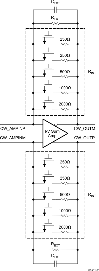 Figure 86. CW Summing Amplifier Block Diagram
Multiple AFE5808A devices are usually utilized in parallel to expand CW beamformer channel count. These AFE5808A devices’ CW outputs can be summed and filtered externally further to achieve desired gain and filter response. AC coupling capacitors CAC are required to block the DC component of the CW carrier signal. CAC can vary from 1 μF to 10 μF depending on the desired low frequency Doppler signal from slow blood flow. Multiple AFE5808A devices’ I/Q outputs can be summed together with a low noise external differential amplifiers before 16/18-bit differential audio ADCs. TI’s ultralow noise differential precision amplifier OPA1632 and THS4130 are suitable devices.
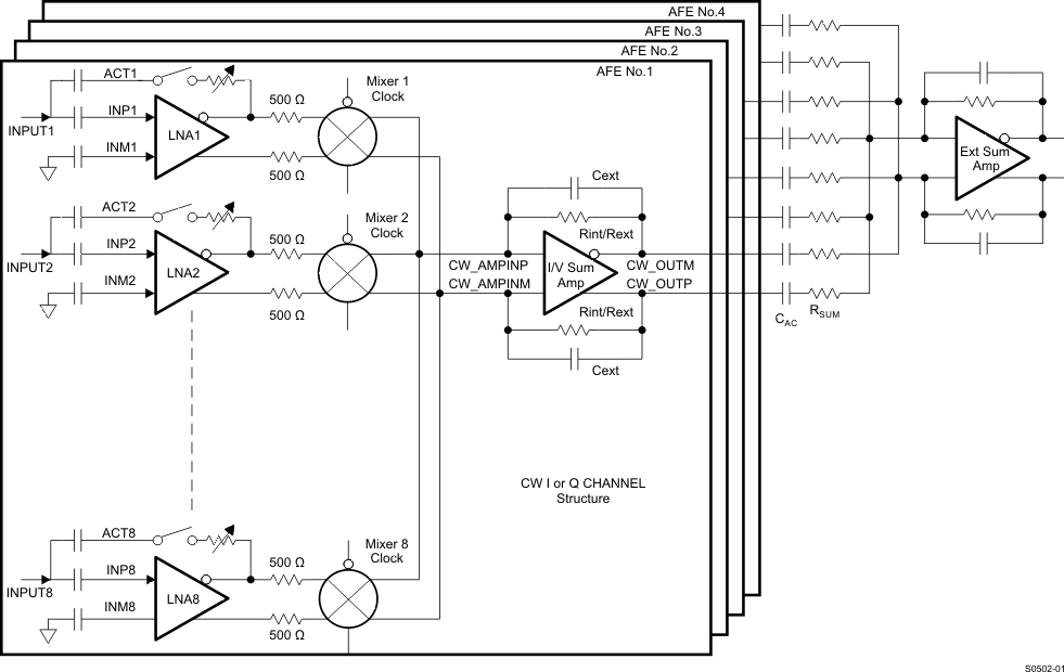 Figure 87. CW Circuit With Multiple AFE5808As
The CW I/Q channels are well matched internally to suppress image frequency components in Doppler spectrum. Low tolerance components and precise operational amplifiers should be used for achieving good matching in the external circuits as well.
NOTE
The local oscillator inputs of the passive mixer are cos(ωt) for I-CH and sin(ωt) for Q-CH respectively. Depending on users' CW Doppler complex FFT processing, swapping I/Q channels in FPGA or DSP may be needed in order to get correct blood flow directions.
9.2.2.3.2 CW Clock Selection
The AFE5808A device can accept differential LVDS, LVPECL, and other differential clock inputs as well as single-ended CMOS clock. An internally generated VCM of 2.5 V is applied to CW clock inputs (that is CLKP_16X/ CLKM_16X and CLKP_1X/ CLKM_1X). Since this 2.5-V VCM is different from the one used in standard LVDS or LVPECL clocks, AC coupling is required between clock drivers and the AFE5808A CW clock inputs. When CMOS clock is used, CLKM_1X and CLKM_16X should be tied to ground. Common clock configurations are shown in Figure 88. To achieve good signal integrity, TI recommends appropriate termination.
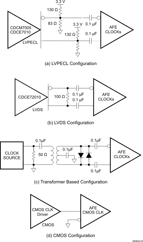 Figure 88. Clock Configurations
The combination of the clock noise and the CW path noise can degrade the CW performance. The internal clocking circuit is designed for achieving excellent phase noise required by CW operation. The phase noise of the AFE5808A CW path is better than 155 dBc/Hz at 1-kHz offset. Consequently the phase noise of the mixer clock inputs needs to be better than 155 dBc/Hz.
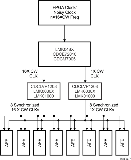
In the 16/8/4 × ƒcw operations modes, low phase noise clock is required for 16/8/4 × ƒcw clocks (that is CLKP_16X/ CLKM_16X pins) to maintain good CW phase noise performance. The 1 × ƒcw clock (that is CLKP_1X/ CLKM_1X pins) is only used to synchronize the multiple AFE5808A chips and is not used for demodulation. Thus 1 × ƒcw clock’s phase noise is not a concern. However, in the 1 × ƒcw operation mode, low phase noise clocks are required for both CLKP_16X/ CLKM_16X and CLKP_1X/ CLKM_1X pins since both of them are used for mixer demodulation. In general, higher slew rate clock has lower phase noise; thus clocks with high amplitude and fast slew rate are preferred in CW operation. In the CMOS clock mode, 5-V CMOS clock can achieve the highest slew rate.
Clock phase noise can be improved by a divider as long as the divider’s phase noise is lower than the target phase noise. The phase noise of a divided clock can be improved approximately by a factor of 20logN dB where N is the dividing factor of 16, 8, or 4. If the target phase noise of mixer LO clock 1׃cw is 160 dBc/Hz at 1 kHz off carrier, the 16 × ƒcw clock phase noise should be better than 160 – 20log16 = 136 dBc/Hz. TI’s jitter cleaners LMK048X/CDCM7005/CDCE72010 exceed this requirement and can be selected for the AFE5808A device. In the 4X/1X modes, higher quality input clocks are expected to achieve the same performance since N is smaller. Thus the 16X mode is a preferred mode since it reduces the phase noise requirement for system clock design. In addition, the phase delay accuracy is specified by the internal clock divider and distribution circuit. In the 16X operation mode, the CW operation range is limited to 8 MHz due to the 16X CLK. The maximum clock frequency for the 16X CLK is 128 MHz. In the 8X, 4X, and 1X modes, higher CW signal frequencies up to 15 MHz can be supported with small degradation in performance (for example, the phase noise is degraded by 9 dB at 15 MHz, compared to 2 MHz).
As the channel number in a system increases, clock distribution becomes more complex. It is not preferred to use one clock driver output to drive multiple AFEs since the clock buffer’s load capacitance increases by a factor of N. As a result, the falling and rising time of a clock signal is degraded. A typical clock arrangement for multiple AFE5808A devices is shown in Figure 89. Each clock buffer output drives one AFE5808A device to achieve the best signal integrity and fastest slew rate, that is better phase noise performance. When clock phase noise is not a concern, for example, the 1 × ƒcw clock in the 16/8/4 × ƒcw operation modes, one clock driver output may excite more than one AFE5808A device. Nevertheless, special considerations must be applied in such a clock distribution network design. In typical ultrasound systems, TI recommends generating all clocks from a same clock source, such as 16 × ƒcw, 1 × ƒcw clocks, audio ADC clocks, RF ADC clock, pulse repetition frequency signal, frame clock, and so forth. By doing this, interference due to clock asynchronization can be minimized.
9.2.2.3.3 CW Supporting Circuits
As a general practice in CW circuit design, in-phase and quadrature channels should be strictly symmetrical by using well matched layout and high accuracy components.
In systems, additional high-pass wall filters (20 Hz to 500 Hz) and low-pass audio filters (10 kHz to 100 kHz) with multiple poles are usually needed. Since CW Doppler signal ranges from 20 Hz to 20 kHz, noise under this range is critical. Consequently low noise audio operational amplifiers are suitable to build these active filters for CW post-processing, for example OPA1632 or OPA2211. More filter design techniques can be found from www.ti.com. TI’s active filter design tool http://www.ti.com/lsds/ti/analog/webench/webench-filters.page.
The filtered audio CW I/Q signals are sampled by audio ADCs and processed by DSP or PC. Although CW signal frequency is from 20 Hz to 20 kHz, higher sampling rate ADCs are still preferred for further decimation and SNR enhancement. Due to the large dynamic range of CW signals, high resolution ADCs (≥ 16 bit) are required, such as ADS8413 (2 MSPS/16 bit/92 dBFS SNR) and ADS8472 (1 MSPS/16 bit/95 dBFS SNR). ADCs for in-phase and quadature-phase channels must be strictly matched, not only amplitude matching but also phase matching, to achieve the best I/Q matching. In addition, the in-phase and quadrature ADC channels must be sampled simultaneously.
9.2.2.4 ADC Operation
9.2.2.4.1 ADC Clock Configurations
To ensure that the aperture delay and jitter are the same for all channels, the AFE5808A device uses a clock tree network to generate individual sampling clocks for each channel. The clock, for all the channels, are matched from the source point to the sampling circuit of each of the eight internal ADCs. The variation on this delay is described in the aperture delay parameter of the output interface timing. Its variation is given by the aperture jitter number of the same table.
The AFE5808A ADC clock input can be driven by differential clocks (sine wave, LVPECL or LVDS) or singled clocks (LVCMOS) similar to CW clocks as shown in Figure 88. In the single-end case, TI recommends using low jitter square signals (LVCMOS levels, 1.8-V amplitude). See the TI technical brief, Clocking High-Speed Data Converters SLYT075 for further details on the theory.
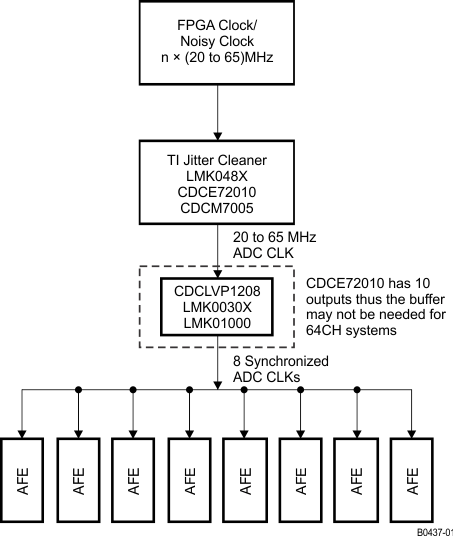
The jitter cleaner LMK048X/CDCM7005/CDCE72010 is suitable to generate the AFE5808A’s ADC clock and ensure the performance for the 14-bit ADC with 77-dBFS SNR. A clock distribution network is shown in Figure 90.
9.2.2.4.2 ADC Reference Circuit
The ADC’s voltage reference can be generated internally or provided externally. When the internal reference mode is selected, the REFP/M becomes output pins and should be floated. When 3[15] = 1 and 1[13] = 1, the device is configured to operate in the external reference mode in which the VREF_IN pin should be driven with a 1.4-V reference voltage and REFP/M must be left open. Since the input impedance of the VREF_IN is high, no special drive capability is required for the 1.4-V voltage reference
The digital beam-forming algorithm in an ultrasound system relies on gain matching across all receiver channels. A typical system would have about 12 octal AFEs on the board. In such a case, it is critical to ensure that the gain is matched, essentially requiring the reference voltages seen by all the AFEs to be the same. Matching references within the eight channels of a chip is done by using a single internal reference voltage buffer. Trimming the reference voltages on each chip during production ensures that the reference voltages are well-matched across different chips. When the external reference mode is used, a solid reference plane on a printed circuit board can ensure minimal voltage variation across devices. More information on voltage reference design can be found in the TI technical brief, How the Voltage Reference Affects ADC Performance, Part 2 (SLYT339). The dominant gain variation in the AFE5808A comes from the VCA gain variation. The gain variation contributed by the ADC reference circuit is much smaller than the VCA gain variation. Hence, in most systems, using the ADC internal reference mode is sufficient to maintain good gain matching among multiple AFE5808As. In addition, the internal reference circuit without any external components achieves satisfactory thermal noise and phase noise performance.
9.2.3 Application Curves
Figure 91 shows the output SNR of one AFE channel from VCNTL = 0 V and VCNTL = 1.2 V, respectively, with an input signal at 5 MHz captured at a sample rate of 50 MHz. VCNTL = 0 V represents far field while VCNTL = 1.2 V represents near field. Figure 92 shows the CW phase noise or dyanmic range of a singe AFE channel.
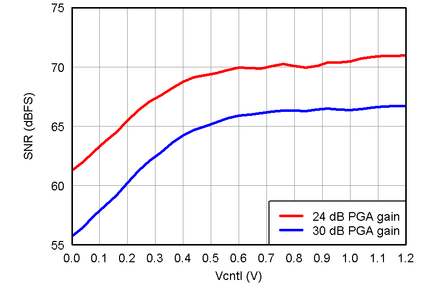 Figure 91. SNR vs VCNTL at 18-dB LNA
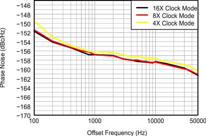 Figure 92. CW Phase Noise at FIN = 2 MHz
9.3 Do's and Don'ts
9.3.1 Driving the Inputs (Analog or Digital) Beyond the Power-Supply Rails
For device reliability, an input must not go more than 300 mV below the ground pins or 300 mV above the supply pins as suggested in the Absolute Maximum Ratings table. Exceeding these limits, even on a transient basis, can cause faulty or erratic operation and can impair device reliability.
9.3.2 Driving the Device Signal Input With an Excessively High Level Signal
The device offers consistent and fast overload recovery with a 6-dB overloaded signal. For very large overload signals (> 6 dB of the linear input signal range), TI recommends back-to-back Schottky clamping diodes at the input to limit the amplitude of the input signal. See the LNA Input Coupling and Decoupling section for more details.
9.3.3 Driving the VCNTL Signal With an Excessive Noise Source
Noise on the VCNTL signal gets directly modulated with the input signal and causes higher output noise and reduction in SNR performance. Maintain a noise level for the VCNTL signal as discussed in the Voltage-Controlled-Attenuator section.
9.3.4 Using a Clock Source With Excessive Jitter, an Excessively Long Input Clock Signal Trace, or Having Other Signals Coupled to the ADC or CW Clock Signal Trace
These situations cause the sampling interval to vary, causing an excessive output noise and a reduction in SNR performance. For a system with multiple devices, the clock tree scheme must be used to apply an ADC or CW clock. See the Switching Characteristics section for clock mismatch between devices, which can lead to latency mismatch and reduction in SNR performance. Clocks generated by FPGA may include excessive jitter and must be evaluated carefully before driving ADC or CW circuits.
9.3.5 LVDS Routing Length Mismatch
The routing length of all LVDS lines routing to the FPGA must be matched to avoid any timing related issue. For systems with multiple devices, the LVDS serialized data clock (DCLKP, DCLKM) and the frame clock (FCLKP, FCLKM) of each individual device must be used to deserialize the corresponding LVDS serialized data (DnP, DnM).
9.3.6 Failure to Provide Adequate Heat Removal
Use the appropriate thermal parameter listed in the Thermal Information table and an ambient, board, or case temperature in order to calculate device junction temperature. A suitable heat removal technique must be used to keep the device junction temperature below the maximum limit of 105°C.
