JAJSHC9B May   2019  – October 2021 ALM2402F-Q1

PRODUCTION DATA  

  1. 特長
  2. アプリケーション
  3. 概要
  4. Revision History
  5. Pin Configuration and Functions
  6. Specifications
    1. 6.1 Absolute Maximum Ratings
    2. 6.2 ESD Ratings
    3. 6.3 Recommended Operating Conditions
    4. 6.4 Thermal Information
    5. 6.5 Electrical Characteristics: VS = 12 V
    6. 6.6 Electrical Characteristics: VS = 5 V
    7. 6.7 Typical Characteristics
  7. Detailed Description
    1. 7.1 Overview
    2. 7.2 Functional Block Diagram
    3. 7.3 Feature Description
      1. 7.3.1 OTF/SH_DN
      2. 7.3.2 Output Stage Supply Voltage
      3. 7.3.3 Current-Limit and Short-Circuit Protection
      4. 7.3.4 Input Common-Mode Overvoltage Clamps
      5. 7.3.5 Thermal Shutdown
      6. 7.3.6 Output Stage
      7. 7.3.7 EMI Susceptibility and Input Filtering
    4. 7.4 Device Functional Modes
      1. 7.4.1 Open-Loop and Closed-Loop Operation
      2. 7.4.2 Shutdown
  8. Application and Implementation
    1. 8.1 Application Information
      1. 8.1.1 Capacitive Load and Stability
    2. 8.2 Typical Application
      1. 8.2.1 Design Requirements
      2. 8.2.2 Detailed Design Procedure
        1. 8.2.2.1 Resolver Excitation Input (Op Amp Output)
          1. 8.2.2.1.1 Excitation Voltage
          2. 8.2.2.1.2 Excitation Frequency
          3. 8.2.2.1.3 Excitation Impedance
        2. 8.2.2.2 Resolver Output
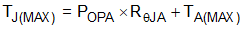
        3. 8.2.2.3 Power Dissipation and Thermal Reliability
          1. 8.2.2.3.1 Improving Package Thermal Performance
      3. 8.2.3 Application Curves
  9. Power Supply Recommendations
  10. 10Layout
    1. 10.1 Layout Guidelines
    2. 10.2 Layout Example
  11. 11Device and Documentation Support
    1. 11.1 Documentation Support
      1. 11.1.1 Related Documentation
    2. 11.2 Receiving Notification of Documentation Updates
    3. 11.3 サポート・リソース
    4. 11.4 Trademarks
    5. 11.5 Electrostatic Discharge Caution
    6. 11.6 Glossary
  12. 12Mechanical, Packaging, and Orderable Information

パッケージ・オプション

メカニカル・データ(パッケージ|ピン)
サーマルパッド・メカニカル・データ
発注情報

Power Dissipation and Thermal Reliability

Power dissipation is critical to many industrial and automotive applications. Resolvers are typically chosen over other position feedback techniques because of reliability and accuracy in harsh conditions and high temperatures.

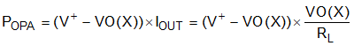
The ALM2402F-Q1 is capable of high output current with power-supply voltages up to 16 V. Internal power dissipation increases when operating at high supply voltages. The power dissipated in the op amp (POPA) is calculated using Equation 6:

Equation 6. GUID-2B01E530-7917-4959-A803-82E5BAAF0A20-low.gif

To calculate the worst-case power dissipation in the op amp, the ac and dc cases must be considered separately.

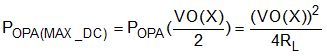
In the case of constant output current (dc) to a resistive load, the maximum power dissipation in the op amp occurs when the output voltage is half the positive supply voltage. This calculation assumes that the op amp is sourcing current from the positive supply to a grounded load. If the op amp sinks current from a grounded load, modify Equation 7 to include the negative supply voltage instead of the positive.

Equation 7. GUID-467E3576-DBC9-4A78-85E7-88F6159C9E7D-low.gif

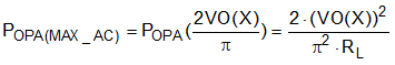
The maximum power dissipation in the op amp for a sinusoidal output current (ac) to a resistive load occurs when the peak output voltage is 2/π times the supply voltage, given symmetrical supply voltages, as shown in Equation 8:

Equation 8. GUID-F5D9B86E-CE38-45CA-843C-E02D1E2FFB62-low.gif

After the total power dissipation is determined, the junction temperature at the worst expected ambient temperature case must be determined by using Equation 9:

Equation 9. GUID-785A82DE-8909-4026-A493-0E378B1840D7-low.gif