JAJSIJ6F April 2011 – February 2020 AMC1204
PRODUCTION DATA.
- 1 特長
- 2 アプリケーション
- 3 概要
- 4 改訂履歴
- 5 概要(続き)
- 6 Pin Configuration and Functions
-
7 Specifications
- 7.1 Absolute Maximum Ratings
- 7.2 ESD Ratings
- 7.3 Recommended Operating Conditions
- 7.4 Thermal Information
- 7.5 Power Ratings
- 7.6 Insulation Specifications
- 7.7 Safety-Related Certifications
- 7.8 Safety Limiting Values
- 7.9 Electrical Characteristics
- 7.10 Timing Requirements
- 7.11 Insulation Characteristics Curves
- 7.12 Typical Characteristics
- 8 Detailed Description
- 9 Application and Implementation
- 10Power Supply Recommendations
- 11Layout
- 12デバイスおよびドキュメントのサポート
- 13メカニカル、パッケージ、および注文情報
パッケージ・オプション
メカニカル・データ(パッケージ|ピン)
サーマルパッド・メカニカル・データ
- DW|16
発注情報
9.1.1 Digital Filter Usage
The modulator generates a bit stream that is processed by a digital filter to obtain a digital word similar to a conversion result of a conventional analog-to-digital converter (ADC). A very simple filter, built with minimal effort and hardware, is a sinc3-type filter, as shown in Equation 1:

This filter provides the best output performance at the lowest hardware size (count of digital gates). For an oversampling rate (OSR) in the range of 16 to 256, this filter is a good choice. All the characterization in this document is also done with a sinc3 filter with OSR = 256 and an output word width of 16 bits.
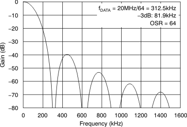
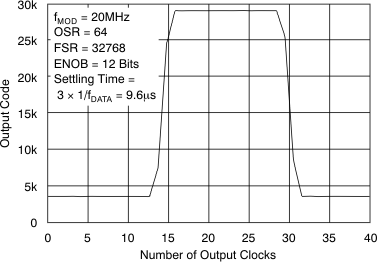
In a sinc3 filter response (shown in Figure 48 and Figure 49), the location of the first notch occurs at the frequency of output data rate fDATA = fCLK/OSR. The –3-dB point is located at half the Nyquist frequency or fDATA/4. For some applications, it may be necessary to use another filter type with different frequency response. Performance can be improved, for example, by using a cascaded filter structure. The first decimation stage could be built of a sinc3 filter with a low OSR and the second stage using a high-order filter.


The effective number of bits (ENOB) is often used to compare the performance of ADCs and ΔΣ modulators. Figure 51 illustrates the ENOB of the AMC1204 and AMC1204B with different oversampling ratios. In this data sheet, this number is calculated from SNR using Equation 2:

An example code for an implementation of a sinc3 filter in an FPGA follows. For more information, see the Combining ADS1202 with FPGA Digital Filter for Current Measurement in Motor Control Applications application note, available for download at www.ti.com.
library IEEE;
use IEEE.std_logic_1164.all;
use IEEE.std_logic_unsigned.all;

entity FLT is
  port(RESN, MOUT, MCLK, CNR : in std_logic;
       CN5 : out std_logic_vector(23 downto 0));
end FLT;

architecture RTL of FLT is
  signal DN0, DN1, DN3, DN5 : std_logic_vector(23 downto 0);
  signal CN1, CN2, CN3, CN4 : std_logic_vector(23 downto 0);
  signal DELTA1 : std_logic_vector(23 downto 0);
begin

process(MCLK, RESn)
  begin
    if RESn = '0' then
      DELTA1 <= (others => '0');
    elsif MCLK'event and MCLK = '1' then
      if MOUT = '1' then
        DELTA1 <= DELTA1 + 1;
      end if;
    end if;
  end process;

process(RESN, MCLK)
  begin
    if RESN = '0' then
      CN1 <= (others => '0');
      CN2 <= (others => '0');
    elsif MCLK'event and MCLK = '1' then
      CN1 <= CN1 + DELTA1;
      CN2 <= CN2 + CN1;
    end if;
  end process;

process(RESN, CNR)
  begin
    if RESN = '0' then
      DN0 <= (others => '0');
      DN1 <= (others => '0');
      DN3 <= (others => '0');
      DN5 <= (others => '0');
    elsif CNR'event and CNR = '1' then
      DN0 <= CN2;
      DN1 <= DN0;
      DN3 <= CN3;
      DN5 <= CN4;
    end if;
  end process;

CN3 <= DN0 - DN1;
CN4 <= CN3 - DN3;
CN5 <= CN4 - DN5;

end RTL;