JAJSE06A October   2017  – December 2017

PRODUCTION DATA.  

  1. 特長
  2. アプリケーション
  3. 概要
    1.     代表的なアプリケーション回路
  4. 改訂履歴
  5. 概要(続き)
  6. Device Comparison Table
  7. Pin Configuration and Functions
    1.     Pin Functions
    2. 7.1 EN1/EN2 Settings
  8. Specifications
    1. 8.1 Absolute Maximum Ratings
    2. 8.2 ESD Ratings
    3. 8.3 Recommended Operating Conditions
    4. 8.4 Thermal Information
    5. 8.5 Dissipation Ratings
    6. 8.6 Electrical Characteristics
    7. 8.7 Typical Characteristics
  9. Detailed Description
    1. 9.1 Overview
    2. 9.2 Functional Block Diagram
    3. 9.3 Feature Description
      1. 9.3.1 Undervoltage Lockout (UVLO)
      2. 9.3.2 Power On
      3. 9.3.3 Overvoltage Protection (OVP)
      4. 9.3.4 Dynamic Power-Path Management
        1. 9.3.4.1 Input Source Connected (ADAPTER or USB)
          1. 9.3.4.1.1 Input DPM Mode (VIN-DPM)
          2. 9.3.4.1.2 DPPM Mode
          3. 9.3.4.1.3 Battery Supplement Mode
        2. 9.3.4.2 Input Source Not Connected
      5. 9.3.5 Battery Charging
        1. 9.3.5.1 Charge Current Translator
        2. 9.3.5.2 Battery Detection and Recharge
        3. 9.3.5.3 Battery Disconnect (SYSOFF Input, bq24076, bq24078)
        4. 9.3.5.4 Dynamic Charge Timers (TMR Input)
        5. 9.3.5.5 Status Indicators (PGOOD, CHG)
        6. 9.3.5.6 Thermal Regulation and Thermal Shutdown
      6. 9.3.6 Battery Pack Temperature Monitoring
    4. 9.4 Device Functional Modes
      1. 9.4.1 Sleep Mode
      2. 9.4.2 Explanation of Deglitch Times and Comparator Hysteresis
  10. 10Application and Implementation
    1. 10.1 Application Information
    2. 10.2 Typical Application
      1. 10.2.1 Design Requirements
      2. 10.2.2 Detailed Design Procedure
        1. 10.2.2.1 bq2407x Charger Design Example
          1. 10.2.2.1.1 System ON/OFF (SYSOFF) (bq24076 or bq24078 only)
        2. 10.2.2.2 Calculations
          1. 10.2.2.2.1 Program the Fast Charge Current (ISET):
          2. 10.2.2.2.2 Program the Input Current Limit (ILIM)
          3. 10.2.2.2.3 Program 6.25-hour Fast-Charge Safety Timer (TMR)
        3. 10.2.2.3 TS Function
        4. 10.2.2.4 CHG and PGOOD
        5. 10.2.2.5 Selecting IN, OUT, and BAT Pin Capacitors
      3. 10.2.3 Application Curves
  11. 11Power Supply Recommendations
  12. 12Layout
    1. 12.1 Layout Guidelines
    2. 12.2 Layout Example
    3. 12.3 Thermal Considerations
  13. 13デバイスおよびドキュメントのサポート
    1. 13.1 デバイス・サポート
      1. 13.1.1 デベロッパー・ネットワークの製品に関する免責事項
    2. 13.2 関連リンク
    3. 13.3 ドキュメントの更新通知を受け取る方法
    4. 13.4 コミュニティ・リソース
    5. 13.5 商標
    6. 13.6 静電気放電に関する注意事項
    7. 13.7 Glossary
  14. 14メカニカル、パッケージ、および注文情報

パッケージ・オプション

メカニカル・データ(パッケージ|ピン)
サーマルパッド・メカニカル・データ
発注情報

Battery Charging

Set CE low to initiate battery charging. First, the device checks for a short-circuit on the BAT pin by sourcing IBAT(SC) to the battery and monitoring the voltage. When the BAT voltage exceeds VBAT(SC), the battery charging continues. The battery is charged in three phases: conditioning pre-charge, constant current fast charge (current regulation) and a constant voltage tapering (voltage regulation). In all charge phases, an internal control loop monitors the IC junction temperature and reduces the charge current if an internal temperature threshold is exceeded.

Figure 17 illustrates a normal Li-Ion charge cycle using the bq2407x:
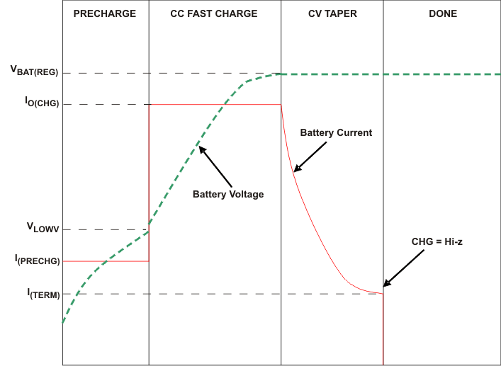
bq24076 bq24078 three_phase_lus810.gifFigure 17. Typical Charge Cycle

In the pre-charge phase, the battery is charged at with the pre-charge current (IPRECHG). Once the battery voltage crosses the VLOWV threshold, the battery is charged with the fast-charge current (ICHG). As the battery voltage reaches VBAT(REG), the battery is held at a constant voltage of VBAT(REG) and the charge current tapers off as the battery approaches full charge. When the battery current reaches ITERM, the CHG pin indicates charging done by going high-impedance.

Note that termination detection is disabled whenever the charge rate is reduced because of the actions of the thermal loop, the DPPM loop or the VIN(LOW) loop.

The value of the fast-charge current is set by the resistor connected from the ISET pin to VSS, and is given by the equation:

Equation 2. ICHG = KISET/RISET

The charge current limit is adjustable up to 1.5 A. The valid resistor range is 590 Ω to 5.9 kΩ. If ICHG is programmed as greater than the input current limit, the battery will not charge at the rate of ICHG, but at the slower rate of IIN(MAX) (minus the load current on the OUT pin, if any). In this case, the charger timers will be proportionately slowed down.