JAJSJH4D december 2010 – september 2020 BQ24133
PRODUCTION DATA
- 1
- 1 特長
- 2 アプリケーション
- 3 概要
- 4 Revision History
- 5 Description (continued)
- 6 Device Comparison Table
- 7 Pin Configuration and Functions
- 8 Specifications
-
9 Detailed Description
- 9.1 Overview
- 9.2 Functional Block Diagram
- 9.3
Feature Description
- 9.3.1 Battery Voltage Regulation
- 9.3.2 Battery Current Regulation
- 9.3.3 Battery Precharge Current Regulation
- 9.3.4 Input Current Regulation
- 9.3.5 Charge Termination, Recharge, And Safety Timers
- 9.3.6 Power Up
- 9.3.7 Input Undervoltage Lockout (UVLO)
- 9.3.8 Input Overvoltage/Undervoltage Protection
- 9.3.9 Enable and Disable Charging
- 9.3.10 System Power Selector
- 9.3.11 Converter Operation
- 9.3.12 Automatic Internal Soft-Start Charger Current
- 9.3.13 Charge Overcurrent Protection
- 9.3.14 Charge Undercurrent Protection
- 9.3.15 Battery Detection
- 9.3.16 Battery Short Protection
- 9.3.17 Battery Overvoltage Protection
- 9.3.18 Temperature Qualification
- 9.3.19 MOSFET Short Circuit and Inductor Short Circuit Protection
- 9.3.20 Thermal Regulation and Shutdown Protection
- 9.3.21 Timer Fault Recovery
- 9.3.22 Charge Status Outputs
- 9.4 Device Functional Modes
- 10Application and Implementation
- 11Power Supply Recommendations
- 12Layout
- 13Device and Documentation Support
- 14Mechanical, Packaging, and Orderable Information
パッケージ・オプション
メカニカル・データ(パッケージ|ピン)
- RGY|24
サーマルパッド・メカニカル・データ
- RGY|24
発注情報
10.2.2.3 Output Capacitor
The output capacitor also should have enough ripple current rating to absorb output switching ripple current. The output capacitor RMS current ICOUT is given as:

The output capacitor voltage ripple can be calculated as follows:
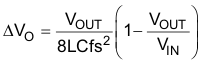
At certain input/output voltages and switching frequencies, the voltage ripple can be reduced by increasing the output filter LC.
The BQ24133 has an internal loop compensator. To achieve good loop stability, the resonant frequency of the output inductor and output capacitor should be designed from 15 kHz to 25 kHz. The preferred ceramic capacitor has a 25-V or higher rating, X7R or X5R.