JAJSBJ1B July 2010 – January 2020 BQ24650
PRODUCTION DATA.
- 1 特長
- 2 アプリケーション
- 3 概要
- 4 改訂履歴
- 5 概要(続き)
- 6 Pin Configuration and Functions
- 7 Specifications
-
8 Detailed Description
- 8.1 Overview
- 8.2 Functional Block Diagram
- 8.3
Feature Description
- 8.3.1 Battery Voltage Regulation
- 8.3.2 Input Voltage Regulation
- 8.3.3 Battery Current Regulation
- 8.3.4 Battery Precharge
- 8.3.5 Charge Termination and Recharge
- 8.3.6 Power Up
- 8.3.7 Enable and Disable Charging
- 8.3.8 Automatic Internal Soft-Start Charger Current
- 8.3.9 Converter Operation
- 8.3.10 Synchronous and Non-Synchronous Operation
- 8.3.11 Cycle-by-Cycle Charge Undercurrent
- 8.3.12 Input Overvoltage Protection (ACOV)
- 8.3.13 Input Undervoltage Lockout (UVLO)
- 8.3.14 Battery Overvoltage Protection
- 8.3.15 Cycle-by-Cycle Charge Overcurrent Protection
- 8.3.16 Thermal Shutdown Protection
- 8.3.17 Temperature Qualification
- 8.3.18 Charge Enable
- 8.3.19 Inductor, Capacitor, and Sense Resistor Selection Guidelines
- 8.3.20 Charge Status Outputs
- 8.3.21 Battery Detection
- 8.4 Device Functional Modes
- 9 Application and Implementation
- 10Power Supply Recommendations
- 11Layout
- 12デバイスおよびドキュメントのサポート
- 13メカニカル、パッケージ、および注文情報
パッケージ・オプション
メカニカル・データ(パッケージ|ピン)
- RVA|16
サーマルパッド・メカニカル・データ
- RVA|16
発注情報
9.2.2.5 Input Filter Design
During adapter hot plug-in, the parasitic inductance and the input capacitor from the adapter cable form a second order system. The voltage spike at the VCC pin may be beyond the IC maximum voltage rating and damage the IC. The input filter must be carefully designed and tested to prevent an overvoltage event on the VCC pin.
There are several methods to damping or limiting the over-voltage spike during adapter hot plug-in. An electrolytic capacitor with high ESR as an input capacitor can damp the overvoltage spike well below the IC maximum pin voltage rating. A high current capability TVS Zener diode can also limit the over-voltage level to an IC safe level. However, these two solutions may not be lowest cost or smallest size.
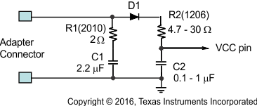
A cost-effective and small size solution is shown in Figure 16. R1 and C1 are composed of a damping RC network to damp the hot plug-in oscillation. As a result, the overvoltage spike is limited to a safe level. D1 is used for reverse voltage protection for the VCC pin. C2 is the VCC pin decoupling capacitor and it must be placed as close as possible to the VCC pin. R2 and C2 form a damping RC network to further protect the IC from high dv/dt and high voltage spike. The C2 value must be less than the C1 value so R1 can dominant the equivalent ESR value to get enough damping effect for hot plug-in. R1 and R2 must be sized enough to handle in-rush current power loss according to the resistor manufacturer’s datasheet. The filter component values always need to be verified with a real application. Table 3 lists the components for the typical application.
 Figure 16. Input Filter
 Table 3. Component List for the Typical System Circuit in Figure 15
| PART DESIGNATOR | QTY | DESCRIPTION |
|---|---|---|
| Q1, Q2 | 2 | N-channel MOSFET, 40-V, 10-A, PowerPAK SO-8, Vishay-Siliconix, Si7288 |
| D2 | 1 | Diode, Dual Schottky, 30-V, 200-mA, SOT-23, Fairchild, BAT54C |
| D3, D4 | 2 | LED Diode, Green, 2.1-V, 20-mA, LTST-C190GKT |
| RSR | 1 | Sense Resistor, 20-mΩ, Vishay-Dale, WSL1206R0200DEA |
| L1 | 1 | Inductor, 10-µH, 7-A, Vishay-Dale IHLP-2525CZ |
| C6, C8 | 2 | Capacitor, Ceramic, 10-μF, 35-V, 20%, X7R, 1210, Panasonic |
| C9 | 1 | Capacitor, Ceramic, 4.7-μF, 35-V, 20%, X7R, 1210, Panasonic |
| C2, C3, C4 | 3 | Capacitor, Ceramic, 1-μF, 35-V, 10%, X7R, 0805, Kemet |
| C5, C7 | 2 | Capacitor, Ceramic, 0.1-μF, 35-V, 10%, X7R, 0805, Kemet |
| C1 | 1 | Capacitor, Ceramic, 2.2-μF, 35-V, 10%, X7R, 1210, Kemet |
| C10 | 1 | Capacitor, Ceramic, 22-pF, 35-V, 10%, X7R, 0603 Kemet |
| R1 | 1 | Resistor, Chip, 100-kΩ, 1/16-W, 0.5%, 0402 |
| R2, R3 | 2 | Resistor, Chip, 499-kΩ, 1/16-W, 0.5%, 0402 |
| R4 | 1 | Resistor, Chip, 36-kΩ, 1/16-W, 0.5%, 0402 |
| R9 | 1 | Resistor, Chip, 5.23-kΩ, 1/16-W, 1%, 0402 |
| R10 | 1 | Resistor, Chip, 30.1-kΩ, 1/16-W, 1%, 0402 |
| R7, R8 | 2 | Resistor, Chip, 10-kΩ, 1/16-W, 5%, 0402 |
| R6 | 1 | Resistor, Chip, 10-Ω, 1/4-W, 5%, 1206 |
| R5 | 1 | Resistor, Chip, 2-Ω, 1-W, 5%, 2012 |
| D1 | 1 | Diode, Schottky Rectifier, 40-V, 10-A, PDS1040 |
| Q3 | 1 | N-Channel MOSFET, 60-V, 115-mA, SOT-23, 2N7002DICT |