SLUS920A July 2009 – July 2015
PRODUCTION DATA.
- 1 Features
- 2 Applications
- 3 Description
- 4 Revision History
- 5 Description (continued)
- 6 Pin Configuration and Functions
- 7 Specifications
-
8 Detailed Description
- 8.1 Overview
- 8.2 Functional Block Diagram
- 8.3
Feature Description
- 8.3.1 Battery Voltage Regulation
- 8.3.2 Battery Current Regulation
- 8.3.3 Input Adapter Current Regulation
- 8.3.4 Adapter Detect and Power Up
- 8.3.5 Enable and Disable Charging
- 8.3.6 System Power Selector
- 8.3.7 Battery Learn Cycles
- 8.3.8 Automatic Internal Soft-Start Charger Current
- 8.3.9 Converter Operation
- 8.3.10 Synchronous and Non-Synchronous Operation
- 8.3.11 High Accuracy IADAPT Using Current Sense Amplifier (CSA)
- 8.3.12 Input Overvoltage Protection (ACOV)
- 8.3.13 Input Undervoltage Lockout (UVLO)
- 8.3.14 AC Lowvoltage (ACLOWV)
- 8.3.15 Battery Overvoltage Protection
- 8.3.16 Battery Shorted (Battery Undervoltage) Protection
- 8.3.17 Charge Overcurrent Protection
- 8.3.18 Thermal Shutdown Protection
- 8.3.19 Adapter Detected Status Register (ACGOOD Pin)
- 8.4 Device Functional Modes
- 9 Application and Implementation
- 10Power Supply Recommendations
- 11Layout
- 12Device and Documentation Support
- 13Mechanical, Packaging, and Orderable Information
パッケージ・オプション
メカニカル・データ(パッケージ|ピン)
- RHD|28
サーマルパッド・メカニカル・データ
- RHD|28
発注情報
11 Layout
11.1 Layout Guidelines
- It is critical that the exposed thermal pad on the backside of the IC package be soldered to the PCB ground. Ensure that there are sufficient thermal vias directly under the IC, connecting to the ground plane on the other layers.
- The control stage and the power stage should be routed separately. At each layer, the signal ground and the power ground are connected only at the thermal pad.
- The AC current-sense resistor must be connected to ACP (pin 3) and ACN (pin 2) with a Kelvin contact. The area of this loop must be minimized. An additional 0.1-μF decoupling capacitor for ACN is required to further reduce noise. The decoupling capacitors for these pins should be placed as close to the IC as possible.
- The charge-current sense resistor must be connected to SRP (pin 19), SRN (pin 18) with a Kelvin contact. The area of this loop must be minimized. An additional 0.1-μF decoupling capacitor for SRN is required to further reduce noise. The decoupling capacitors for these pins should be placed as close to the IC as possible.
- Decoupling capacitors for PVCC (pin 28), VREF (pin 10), REGN (pin 24) should be placed underneath the IC (on the bottom layer) with the interconnections to the IC as short as possible.
- Decoupling capacitors for BAT (pin 17), IADAPT (pin 15) must be placed close to the corresponding IC pins with the interconnections to the IC as short as possible.
- Decoupling capacitor CX for the charger input must be placed close to the Q4 drain and Q5 source.
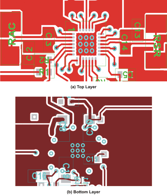
Figure 42 shows the recommended component placement with trace and via locations.
For VQFN information, refer to the following links: SCBA017 and SLUA271.
11.2 Layout Example
 Figure 42. PCB Layout Layers