JAJSGX5C july 2018 – april 2023 BQ25150
PRODUCTION DATA
- 1
- 1 特長
- 2 アプリケーション
- 3 概要
- 4 Revision History
- 5 概要 (続き)
- 6 Device Key Default Settings
- 7 Pin Configuration and Functions
- 8 Specifications
-
9 Detailed Description
- 9.1 Overview
- 9.2 Functional Block Diagram
- 9.3
Feature Description
- 9.3.1 Linear Charger and Power Path
- 9.3.2 Protection Mechanisms
- 9.3.3 ADC
- 9.3.4 VDD LDO
- 9.3.5 Load Switch / LDO Output and Control
- 9.3.6 PMID Power Control
- 9.3.7 MR Wake and Reset Input
- 9.3.8 14-Second Watchdog for HW Reset
- 9.3.9 Faults Conditions and Interrupts ( INT)
- 9.3.10 Power Good ( PG) Pin
- 9.3.11 External NTC Monitoring (TS)
- 9.3.12 External NTC Monitoring (ADCIN)
- 9.3.13 I2C Interface
- 9.4 Device Functional Modes
- 9.5 Register Map
- 10Application and Implementation
- 11Power Supply Recommendations
- 12Layout
- 13Device and Documentation Support
- 14Mechanical, Packaging, and Orderable Information
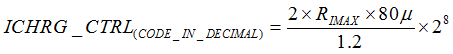
9.3.2.6 Maximum Allowable Charging Current (IMAX)
The device allows the system designer to limit the maximum programmable charge current through hardware by connecting a resistor to the IMAX pin. The value of this resistor will determine the maximum Fast Charge I2C code that BQ25150 would let the host program to the device. Upon Power-On-Reset (POR) the ADC will measure the voltage at the IMAX pin, which is biased by a 80-µA biasing current. This measurement is used to determine the RIMAX value and the maximum charging current. Once the value is measured, the device determines the maximum allowable Fast Charge I2C code and prevents the host from programming any value higher than that. If the host tries to program it to a higher value, the IMAX_ACTIVE flag will be set and the Fast Charge Current Register will reflect the maximum charge current setting instead of the value programmed by the host. Note that even though the pre-charge current is also limited by IMAX if set higher than the IMAX value, the IMAX_ACTIVE flag is not set as it is only asserted for fast charge. Equation 6 shows the maximum ICHG_CTRL register value (decimal) for a given RIMAX.
Note that the IMAX function has no effect on the charge current step size set by the ICHARGE_RANGE bit, so if RIMAX is selected based on the fast charge current when ICHARGE_RANGE = 0 (1.25-mA step), changing the ICHARGE_RANGE bit to 1 will double the maximum allowable current.In case where the IMAX pin is left floating (RIMAX > 14 KΩ,), the device will disable charging so that in the case the IMAX resistor connection is not done properly during manufacturing or breaks afterwards it prevents charging with a current above the desired IMAX level. If the measurement indicates that the IMAX pin is floating, the device repeats the measurement for a second time to confirm. If the floating pin measurement is confirmed then, charge is disabled permanently and the IMAX_FAULT flag is set. Note that a Power-On-Reset (POR) would be needed in order to repeat the IMAX measurement so both IN and BAT supplies must be removed before powering up the device again to update the IMAX state.