JAJSCF8D August 2016 – July 2019 CC2650MODA
PRODUCTION DATA.
- 1 デバイスの概要
- 2 改訂履歴
- 3 Device Comparison
- 4 Terminal Configuration and Functions
-
5 Specifications
- 5.1 Absolute Maximum Ratings
- 5.2 ESD Ratings
- 5.3 Recommended Operating Conditions
- 5.4 Power Consumption Summary
- 5.5 General Characteristics
- 5.6 Antenna
- 5.7 1-Mbps GFSK (Bluetooth low energy) – RX
- 5.8 1-Mbps GFSK (Bluetooth low energy) – TX
- 5.9 IEEE 802.15.4 (Offset Q-PSK DSSS, 250 kbps) – RX
- 5.10 IEEE 802.15.4 (Offset Q-PSK DSSS, 250 kbps) – TX
- 5.11 24-MHz Crystal Oscillator (XOSC_HF)
- 5.12 32.768-kHz Crystal Oscillator (XOSC_LF)
- 5.13 48-MHz RC Oscillator (RCOSC_HF)
- 5.14 32-kHz RC Oscillator (RCOSC_LF)
- 5.15 ADC Characteristics
- 5.16 Temperature Sensor
- 5.17 Battery Monitor
- 5.18 Continuous Time Comparator
- 5.19 Low-Power Clocked Comparator
- 5.20 Programmable Current Source
- 5.21 DC Characteristics
- 5.22 Thermal Resistance Characteristics for MOH Package
- 5.23 Timing Requirements
- 5.24 Switching Characteristics
- 5.25 Typical Characteristics
-
6 Detailed Description
- 6.1 Overview
- 6.2 Functional Block Diagram
- 6.3 Main CPU
- 6.4 RF Core
- 6.5 Sensor Controller
- 6.6 Memory
- 6.7 Debug
- 6.8 Power Management
- 6.9 Clock Systems
- 6.10 General Peripherals and Modules
- 6.11 System Architecture
- 6.12 Certification
- 6.13 End Product Labeling
- 6.14 Manual Information to the End User
- 6.15 Module Marking
- 7 Application, Implementation, and Layout
- 8 Environmental Requirements and Specifications
- 9 デバイスおよびドキュメントのサポート
- 10メカニカル、パッケージ、および注文情報
パッケージ・オプション
デバイスごとのパッケージ図は、PDF版データシートをご参照ください。
メカニカル・データ(パッケージ|ピン)
- MOH|29
サーマルパッド・メカニカル・データ
発注情報
8.5 Soldering and Reflow Condition
- Heating method: Conventional convection or IR convection
- Temperature measurement: Thermocouple d = 0.1 mm to 0.2 mm CA (K) or CC (T) at soldering portion or equivalent method
- Solder paste composition: Sn/3.0 Ag/0.5 Cu
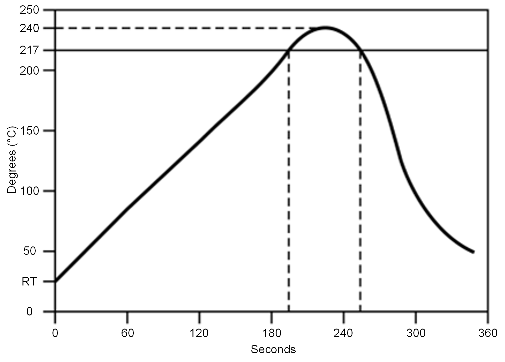
- Allowable reflow soldering times: 2 times based on the reflow soldering profile (see Figure 8-1)
- Temperature profile: Reflow soldering will be done according to the temperature profile
(see Figure 8-1)
 Figure 8-1 Temperature Profile for Evaluation of Solder Heat Resistance of a Component
(at Solder Joint)
Table 8-1 Temperature Profile
| Profile Elements | Convection or IR(1) |
|---|---|
| Peak temperature range | 235 to 240°C typical (260°C maximum) |
| Pre-heat / soaking (150 to 200°C) | 60 to 120 seconds |
| Time above melting point | 60 to 90 seconds |
| Time with 5°C to peak | 30 seconds maximum |
| Ramp up | < 3°C / second |
| Ramp down | < -6°C / second |
(1) For details, refer to the solder paste manufacturer's recommendation.
NOTE
TI does not recommend the use of conformal coating or similar material on the SimpleLink™ module. This coating can lead to localized stress on the solder connections inside the module and impact the module reliability. Use caution during the module assembly process to the final PCB to avoid the presence of foreign material inside the module.