SLPS388B September 2012 – January 2015 CSD18533Q5A
PRODUCTION DATA.
- 1Features
- 2Applications
- 3Description
- 4Revision History
- 5Specifications
- 6Device and Documentation Support
- 7Mechanical, Packaging, and Orderable Information
パッケージ・オプション
デバイスごとのパッケージ図は、PDF版データシートをご参照ください。
メカニカル・データ(パッケージ|ピン)
- DQJ|8
サーマルパッド・メカニカル・データ
発注情報
5 Specifications
5.1 Electrical Characteristics
(TA = 25°C unless otherwise stated)| PARAMETER | TEST CONDITIONS | MIN | TYP | MAX | UNIT | ||
|---|---|---|---|---|---|---|---|
| ¨STATIC CHARACTERISTICS | |||||||
| BVDSS | Drain-to-Source Voltage | VGS = 0 V, ID = 250 μA | 60 | V | |||
| IDSS | Drain-to-Source Leakage Current | VGS = 0 V, VDS = 48 V | 1 | μA | |||
| IGSS | Gate-to-Source Leakage Current | VDS = 0 V, VGS = 20 V | 100 | nA | |||
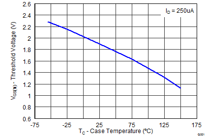
| VGS(th) | Gate-to-Source Threshold Voltage | VDS = VGS, ID = 250 μA | 1.5 | 1.9 | 2.3 | V | |
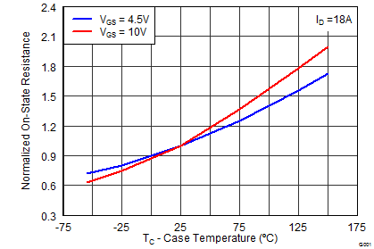
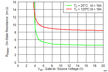
| RDS(on) | Drain-to-Source On-Resistance | VGS = 4.5 V, ID = 18 A | 6.5 | 8.5 | mΩ | ||
| VGS = 10 V, ID = 18 A | 4.7 | 5.9 | mΩ | ||||
| gƒs | Transconductance | VDS = 30 V, ID = 18 A | 122 | S | |||
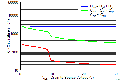
| DYNAMIC CHARACTERISTICS | |||||||
| Ciss | Input Capacitance | VGS = 0 V, VDS = 30 V, ƒ = 1 MHz | 2200 | 2750 | pF | ||
| Coss | Output Capacitance | 292 | 365 | pF | |||
| Crss | Reverse Transfer Capacitance | 7 | 9 | pF | |||
| RG | Series Gate Resistance | 1.3 | 2.6 | Ω | |||
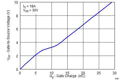
| Qg | Gate Charge Total (4.5 V) | VDS = 30 V, ID = 18 A | 14 | 18 | nC | ||
| Qg | Gate Charge Total (10 V) | 29 | 36 | ||||
| Qgd | Gate Charge Gate-to-Drain | 5.4 | nC | ||||
| Qgs | Gate Charge Gate-to-Source | 6.6 | nC | ||||
| Qg(th) | Gate Charge at Vth | 4.7 | nC | ||||
| Qoss | Output Charge | VDS = 30 V, VGS = 0 V | 31 | nC | |||
| td(on) | Turn On Delay Time | VDS = 30 V, VGS = 10 V, IDS = 18 A, RG = 0 Ω | 5.2 | ns | |||
| tr | Rise Time | 5.5 | ns | ||||
| td(off) | Turn Off Delay Time | 15 | ns | ||||
| tƒ | Fall Time | 2.0 | ns | ||||
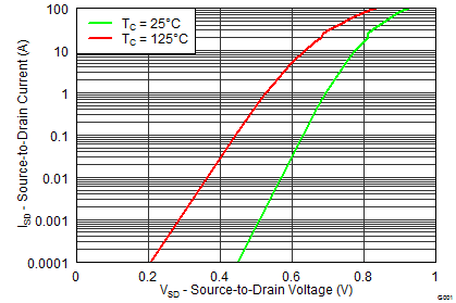
| DIODE CHARACTERISTICS | |||||||
| VSD | Diode Forward Voltage | ISD = 18 A, VGS = 0 V | 0.8 | 1 | V | ||
| Qrr | Reverse Recovery Charge | VDS= 30 V, IF = 18 A, di/dt = 300 A/μs | 68 | nC | |||
| trr | Reverse Recovery Time | 40 | ns | ||||
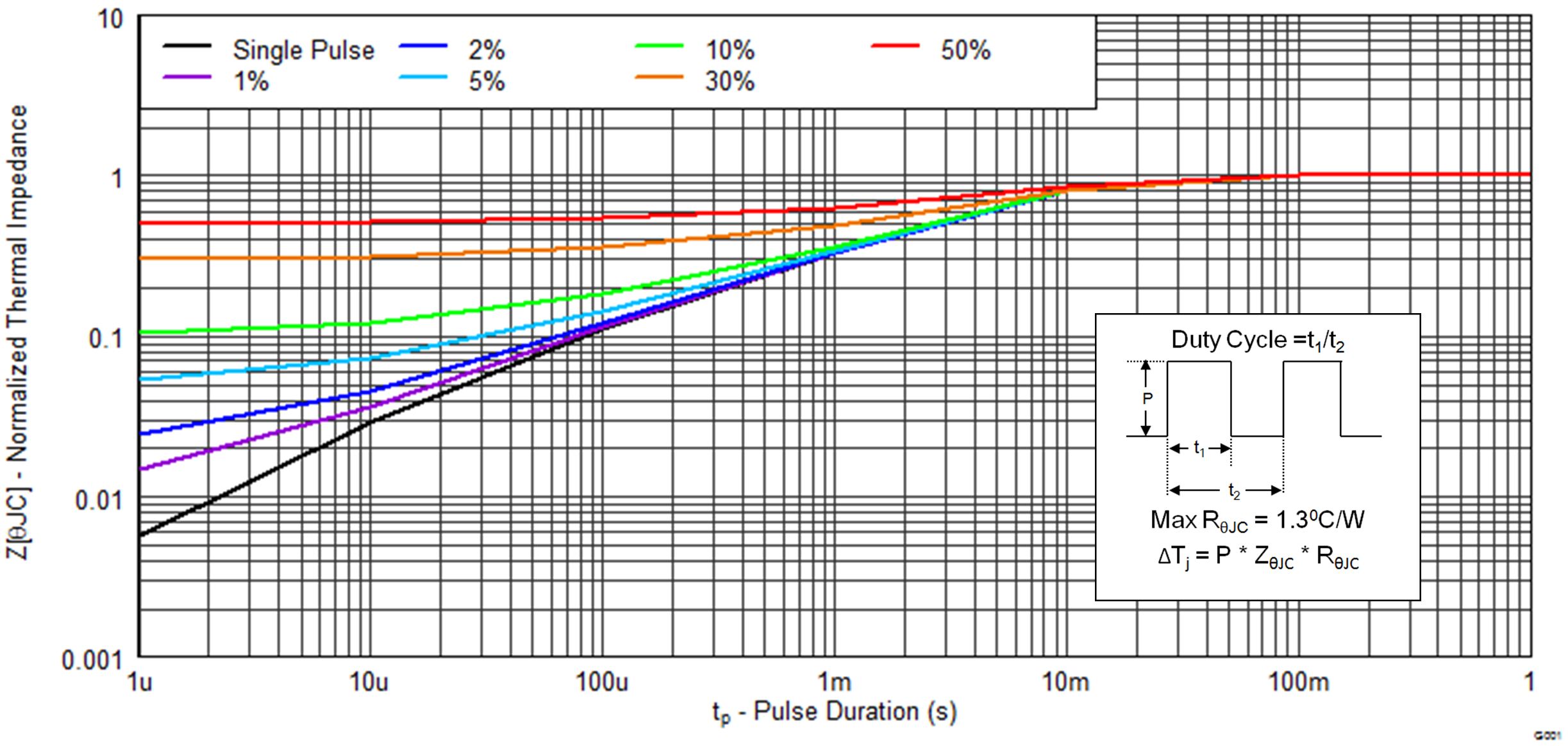
5.2 Thermal Information
(TA = 25°C unless otherwise stated)| THERMAL METRIC | MIN | TYP | MAX | UNIT | |
|---|---|---|---|---|---|
| RθJC | Thermal Resistance Junction to Case(1) | 1.3 | °C/W | ||
| RθJA | Thermal Resistance Junction to Ambient(1)(2) | 50 | |||
(1) RθJC is determined with the device mounted on a 1 inch2 (6.45 cm2), 2 oz. (0.071 mm thick) Cu pad on a 1.5 inch × 1.5 inch (3.81 cm × 3.81 cm), 0.06 inch (1.52 mm) thick FR4 PCB. RθJC is specified by design, whereas RθJA is determined by the user’s board design.
(2) Device mounted on FR4 material with 1 inch2 (6.45 cm2), 2 oz. (0.071 mm thick) Cu.
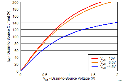
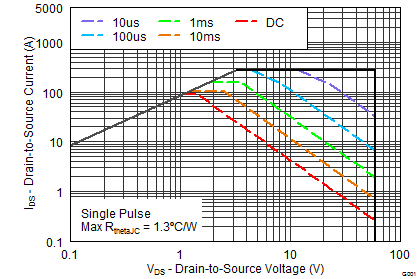
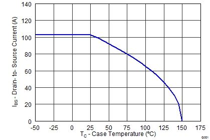
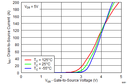
5.3 Typical MOSFET Characteristics
(TA = 25°C unless otherwise stated)