SLPS286D June 2011 – February 2017 CSD87352Q5D
PRODUCTION DATA.
5 Specifications
5.1 Absolute Maximum Ratings
TA = 25°C (unless otherwise noted) (1)| PARAMETER | CONDITIONS | MIN | MAX | UNIT |
|---|---|---|---|---|
| Voltage | VIN to PGND | 30 | V | |
| VSW to PGND | 30 | |||
| VSW to PGND (10 ns) | 32 | |||
| TG to TGR | –8 | 10 | ||
| BG to PGND | –8 | 10 | ||
| Pulsed current rating, IDM(2) | 60 | A | ||
| Power dissipation, PD | 8.5 | W | ||
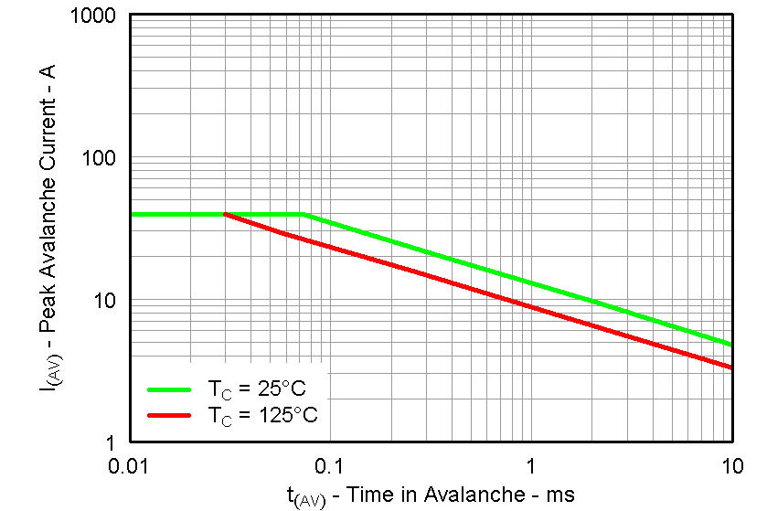
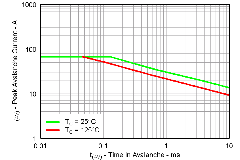
| Avalanche energy, EAS | Sync FET, ID = 65 A, L = 0.1 mH | 211 | mJ | |
| Control FET, ID = 37 A, L = 0.1 mH | 68 | |||
| Operating junction, TJ | –55 | 150 | °C | |
| Storage temperature, TSTG | –55 | 150 | °C | |
(1) Stresses beyond those listed under Absolute Maximum Ratings may cause permanent damage to the device. These are stress ratings only, and functional operation of the device at these or any other conditions beyond those indicated in the Recommended Operating Conditions is not implied. Exposure to absolute-maximum-rated conditions for extended periods may affect device reliability.
5.2 Recommended Operating Conditions
TA = 25°C (unless otherwise noted)| PARAMETER | CONDITIONS | MIN | MAX | UNIT |
|---|---|---|---|---|
| Gate drive voltage, VGS | 4.5 | 8 | V | |
| Input supply voltage, VIN | 27 | V | ||
| Switching frequency, ƒSW | CBST = 0.1 μF (min) | 1500 | kHz | |
| Operating current | 25 | A | ||
| Operating temperature, TJ | 125 | °C | ||
5.3 Power Block Performance
TA = 25°C (unless otherwise noted)| PARAMETER | CONDITIONS | MIN | TYP | MAX | UNIT |
|---|---|---|---|---|---|
| Power loss, PLOSS (1) | VIN = 12 V, VGS = 5 V, VOUT = 1.3 V, IOUT = 15 A, ƒSW = 500 kHz, LOUT = 0.3 µH, TJ = 25°C |
1.8 | W | ||
| VIN quiescent current, IQVIN | TG to TGR = 0 V BG to PGND = 0 V |
10 | µA |
(1) Measurement made with six 10-µF (TDK C3216X5R1C106KT or equivalent) ceramic capacitors placed across VIN to PGND pins and using a high-current 5-V driver IC.
5.4 Thermal Information
TA = 25°C (unless otherwise stated)| THERMAL METRIC | MIN | TYP | MAX | UNIT | |
|---|---|---|---|---|---|
| RθJA | Junction-to-ambient thermal resistance (min Cu)(1)(2) | 150 | °C/W | ||
| Junction-to-ambient thermal resistance (max Cu)(1)(2) | 82 | ||||
| RθJC | Junction-to-case thermal resistance (top of package)(2) | 33 | °C/W | ||
| Junction-to-case thermal resistance (PGND pin)(2) | 2.8 | ||||
(1) Device mounted on FR4 material with 1-in2 (6.45-cm2) Cu.
(2) RθJC is determined with the device mounted on a 1-in2 (6.45-cm2), 2-oz (0.071-mm) thick Cu pad on a 1.5-in × 1.5-in
(3.81-cm × 3.81-cm), 0.06-in (1.52-mm) thick FR4 board. RθJC is specified by design while RθJA is determined by the user’s board design.
(3.81-cm × 3.81-cm), 0.06-in (1.52-mm) thick FR4 board. RθJC is specified by design while RθJA is determined by the user’s board design.
5.5 Electrical Characteristics
TA = 25°C (unless otherwise stated)| PARAMETER | TEST CONDITIONS | Q1 Control FET | Q2 Sync FET | UNIT | ||||||
|---|---|---|---|---|---|---|---|---|---|---|
| MIN | TYP | MAX | MIN | TYP | MAX | |||||
| STATIC CHARACTERISTICS | ||||||||||
| BVDSS | Drain-to-source voltage | VGS = 0 V, IDS = 250 μA | 30 | 30 | V | |||||
| IDSS | Drain-to-source leakage current | VGS = 0 V, VDS = 24 V | 1 | 1 | μA | |||||
| IGSS | Gate-to-source leakage current | VDS = 0 V, VGS = +10 / –8 V | 100 | 100 | nA | |||||
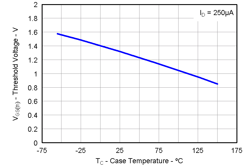
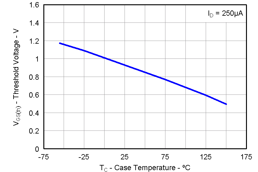
| VGS(th) | Gate-to-source threshold voltage | VDS = VGS, IDS = 250 μA | 1 | 2.1 | 0.75 | 1.15 | V | |||
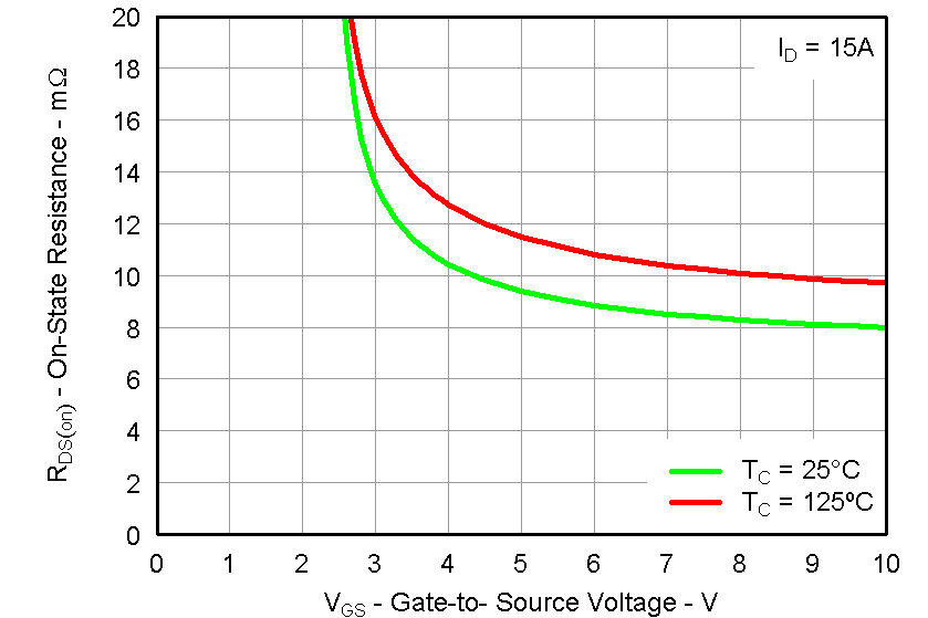
| ZDS(on)(1) | Effective AC on-impedance | VIN = 12 V, VGS = 5 V, VOUT = 1.3 V, IOUT = 15 A, ƒSW = 500 kHz, LOUT = 0.3 µH, TJ = 25°C |
9 | 2.8 | mΩ | |||||
| gfs | Transconductance | VDS = 15 V, IDS = 15 A | 51 | 87 | S | |||||
| DYNAMIC CHARACTERISTICS | ||||||||||
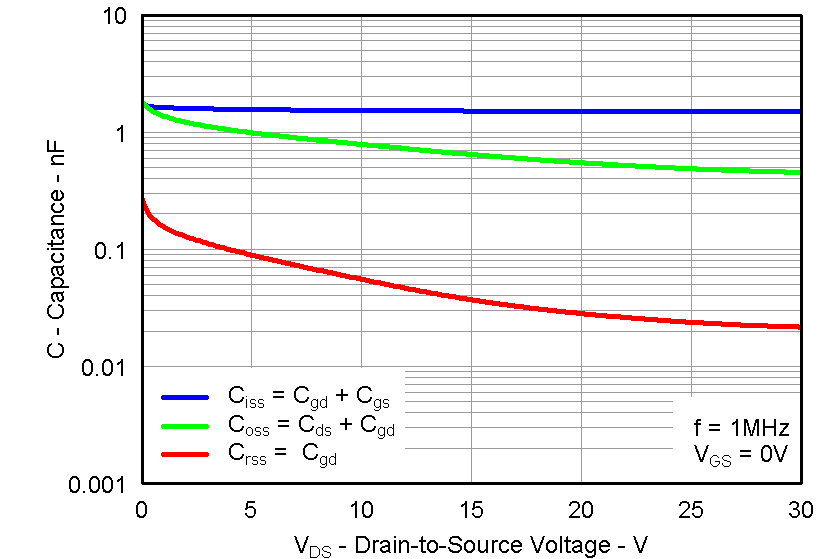
| CISS | Input capacitance | VGS = 0 V, VDS = 15 V, ƒ = 1 MHz |
740 | 890 | 1500 | 1800 | pF | |||
| COSS | Output capacitance | 315 | 380 | 645 | 775 | pF | ||||
| CRSS | Reverse transfer capacitance | 12 | 14 | 38 | 46 | pF | ||||
| RG | Series gate resistance | 1.2 | 2.4 | 0.6 | 1.2 | Ω | ||||
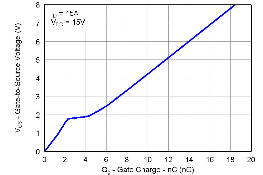
| Qg | Gate charge total (4.5 V) | VDS = 15 V, IDS = 15 A |
4.6 | 5.5 | 10.4 | 12.5 | nC | |||
| Qgd | Gate charge gate-to-drain | 0.9 | 1.9 | nC | ||||||
| Qgs | Gate charge gate-to-source | 1.5 | 2.2 | nC | ||||||
| Qg(th) | Gate charge at Vth | 0.9 | 1.2 | nC | ||||||
| QOSS | Output charge | VDS = 9.8 V, VGS = 0 V | 6.6 | 13 | nC | |||||
| td(on) | Turnon delay time | VDS = 15 V, VGS = 4.5 V, IDS = 15 A, RG = 2 Ω |
5.4 | 6.1 | ns | |||||
| tr | Rise time | 11 | 7 | ns | ||||||
| td(off) | Turnoff delay time | 9.5 | 16 | ns | ||||||
| tf | Fall time | 2 | 2.7 | ns | ||||||
| DIODE CHARACTERISTICS | ||||||||||
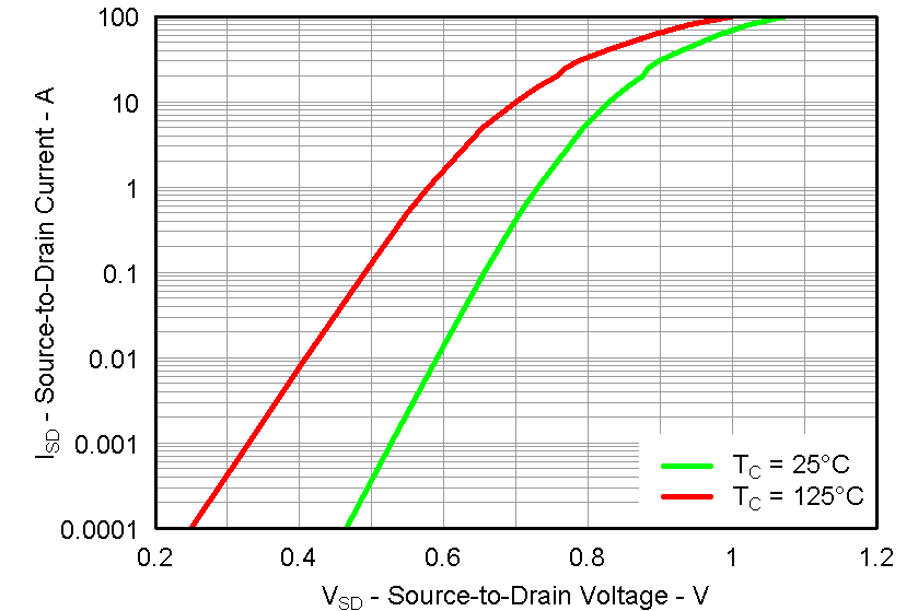
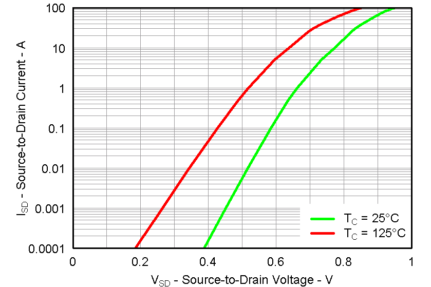
| VSD | Diode forward voltage | IDS = 15 A, VGS = 0 V | 0.8 | 0.8 | V | |||||
| Qrr | Reverse recovery charge | Vdd = 9.8 V, IF = 15 A, di/dt = 300 A/μs |
11.3 | 16.3 | nC | |||||
| trr | Reverse recovery time | 16 | 20 | ns | ||||||
(1) Equivalent system performance based on application testing. See Application and Implementation for details.
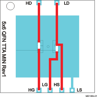 |
Max RθJA = 82°C/W when mounted on 1 in2 (6.45 cm2) of 2-oz (0.071-mm) thick Cu. |
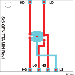 |
Max RθJA = 150°C/W when mounted on minimum pad area of 2-oz (0.071-mm) thick Cu. |
5.6 Typical Power Block Device Characteristics
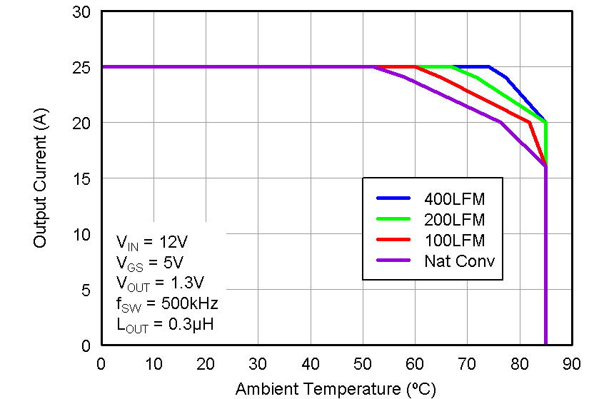
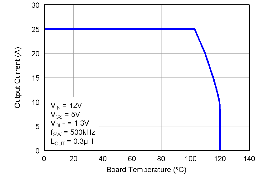
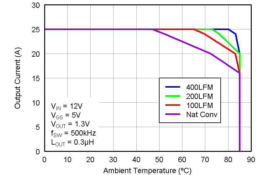
TJ = 125°C, unless stated otherwise.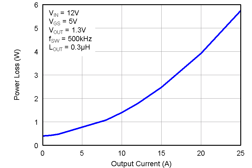
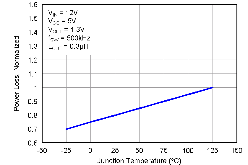
1. The typical power block system characteristic curves are based on measurements made on a PCB design with dimensions of 4 in (W) × 3.5 in (L) x 0.062 in (H) and 6 copper layers of 1-oz copper thickness. See Application and Implementation section for detailed explanation.
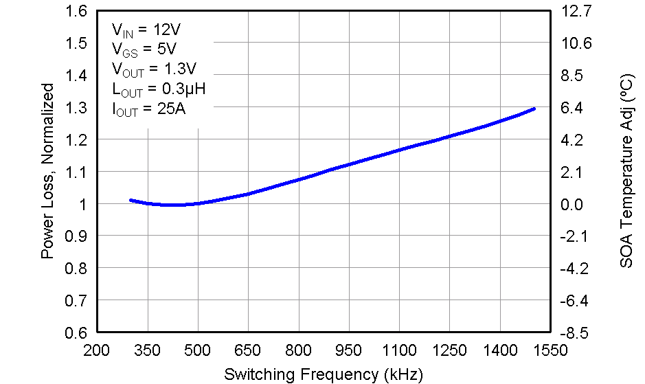
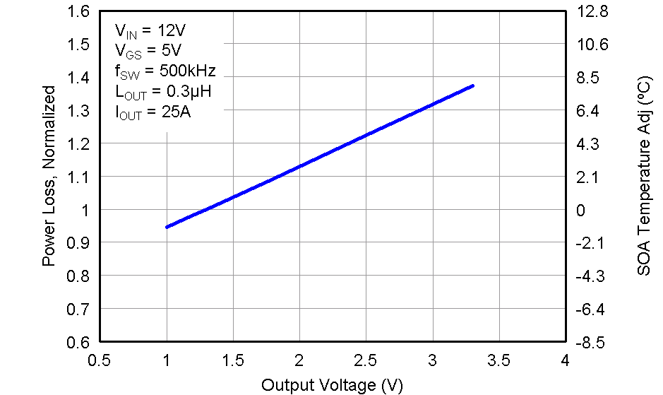
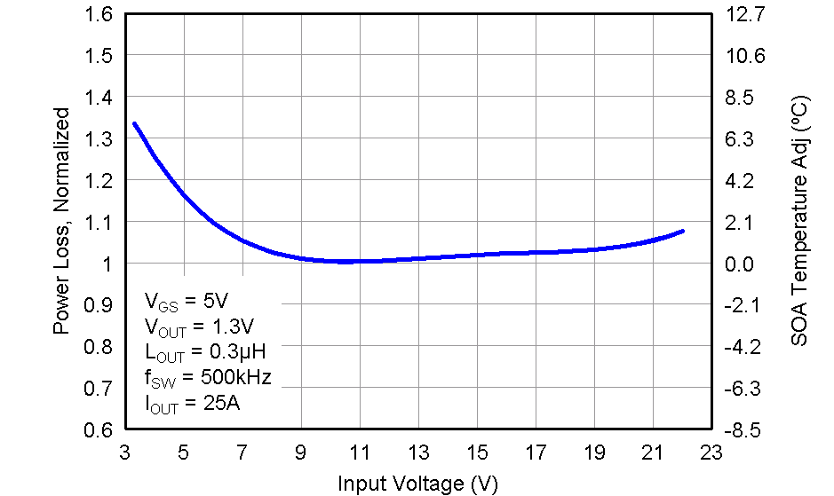
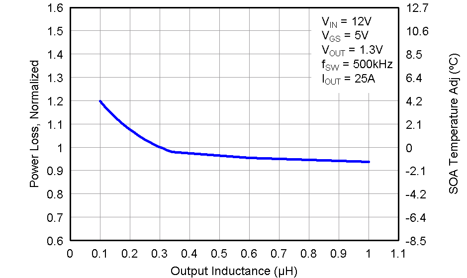
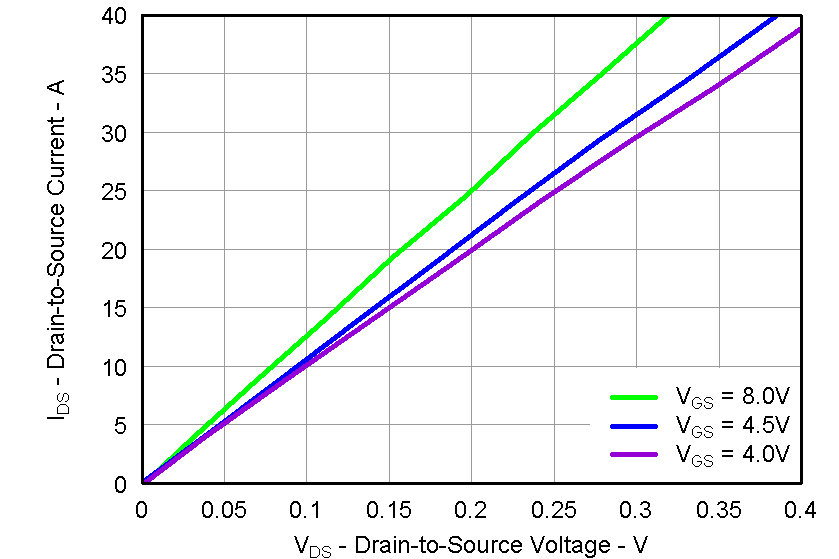
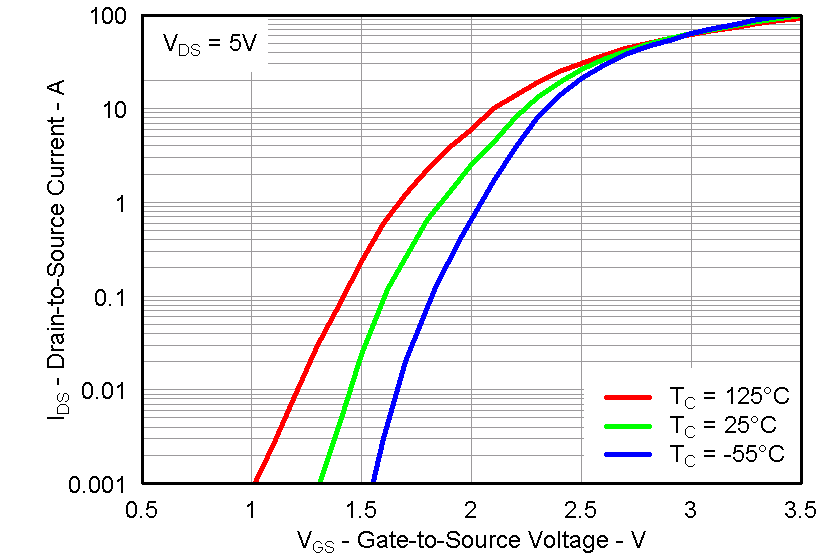
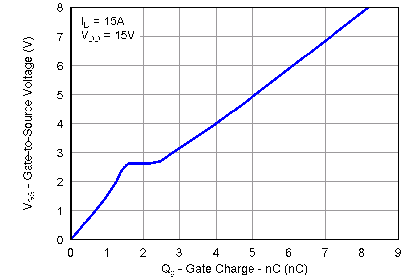
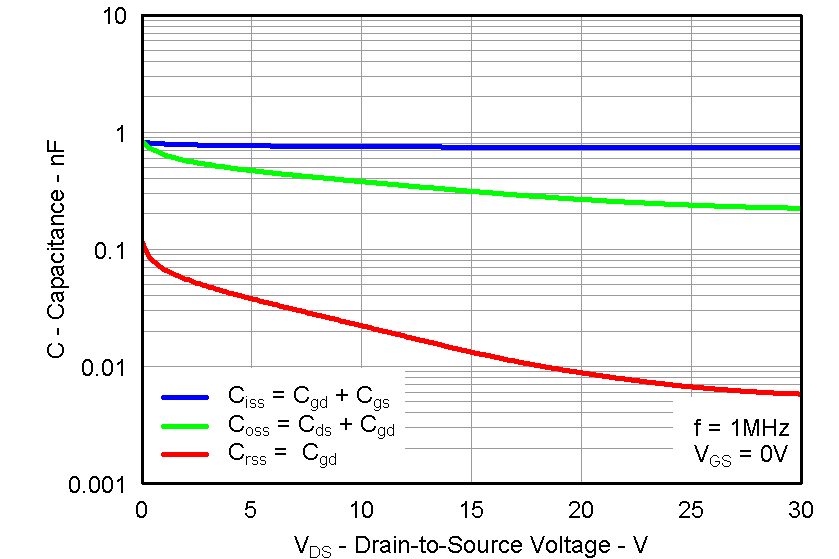
5.7 Typical Power Block MOSFET Characteristics
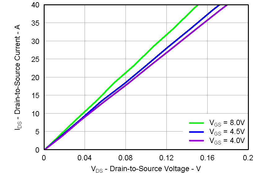
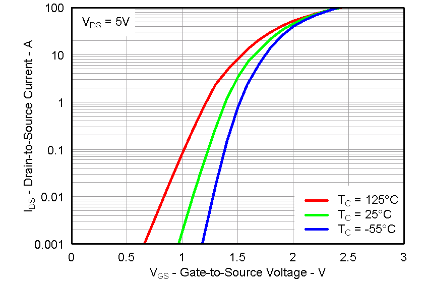
TA = 25°C, unless stated otherwise.