JAJSD35D may 2017 – december 2018 CSD88584Q5DC
PRODUCTION DATA
- 1
- 1特長
- 2アプリケーション
- 3概要
- 4Revision History
- 5Specifications
-
6Application and Implementation
- 6.1 Application Information
- 6.2 Brushless DC Motor With Trapezoidal Control
- 6.3 Power Loss Curves
- 6.4 Safe Operating Area (SOA) Curve
- 6.5 Normalized Power Loss Curves
- 6.6 Design Example – Regulate Current to Maintain Safe Operation
- 6.7 Design Example – Regulate Board and Case Temperature to Maintain Safe Operation
- 7Layout
- 8Device and Documentation Support
- 9Mechanical, Packaging, and Orderable Information
パッケージ・オプション
デバイスごとのパッケージ図は、PDF版データシートをご参照ください。
メカニカル・データ(パッケージ|ピン)
- DMM|22
サーマルパッド・メカニカル・データ
発注情報
6.3 Power Loss Curves
CSD88584Q5DC was designed to operate up to 7-cell Li-Ion battery voltage applications ranging from 18 V to 32 V, typical 24 V. For 8s, input voltages between 32 V to 36 V, RC snubbers are required for each switch-node U, V, and W. To reduce ringing, refer to the Section 7.1.1 section. In an effort to simplify the design process, Texas Instruments has provided measured power loss performance curves over a variety of typical conditions.
Figure 5-1 plots the CSD88584Q5DC power loss as a function of load current. The measured power loss includes both input conversion loss and gate drive loss.
Equation 1 is used to generate the power loss curve:
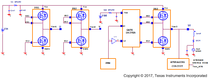
The power loss measurements were made on the circuit shown in Figure 6-3, power block devices for legs U and V, PB1 and PB2 were disabled by shorting the CSD88584Q5DC high-side and low-side FETs gate-to-source terminals. Current shunt Iin_shunt provides Input current and Idd_SHUNT provides driver supply current measurements. The winding current is measured from the DC load. An averaging circuit provides switch node W equivalent RMS voltage.
 Figure 6-3 Power Loss Test Circuit
The RMS current on the CSD88584Q5DC device depends on the motor winding current. For trapezoidal control, the MOSFET RMS current is calculated using Equation 2.
Taking into consideration system tolerances with the current measurement scheme, the inverter design needs to withstand a 20% overload current.
| Winding RMS Current (A) | CSD88584Q5DC IRMS (A) | Overload 120% × IRMS (A) |
|---|---|---|
| 30 | 42 | 51 |
| 40 | 56 | 68 |
| 50 | 70 | 85 |