JAJSJI1E October 2020 – January 2021 DAC5652
PRODUCTION DATA
- 1 特長
- 2 アプリケーション
- 3 概要
- 4 Revision History
- 5 Pin Configuration and Functions
-
6 Specifications
- 6.1 Absolute Maximum Rationgs
- 6.2 ESD Ratings
- 6.3 Recommended Operating Conditions
- 6.4 Thermal Resistance Characteristics
- 6.5 Electrical Characteristics
- 6.6 Electrical Characteristics
- 6.7 Electrical Characteristics, AC
- 6.8 Electrical Characteristics, DC
- 6.9 Switching Characteristics
- 6.10 Typical Characteristics
- 7 Parameter Measurement Information
- 8 Detailed Description
- 9 Application Information Disclaimer
- 10Power Supply Recommendations
- 11Layout
- 12Device and Documentation Support
- 13Mechanical, Packaging, and Orderable Information
パッケージ・オプション
メカニカル・データ(パッケージ|ピン)
- PFB|48
サーマルパッド・メカニカル・データ
- PFB|48
発注情報
11.2 Layout Example
Figure 11-1 through Figure 11-4 show the layout examples.
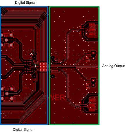 Figure 11-1 Top Layer (Layer 1)
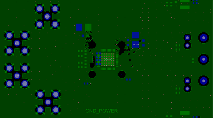 Figure 11-2 Single Ground Plane (Layer
2)
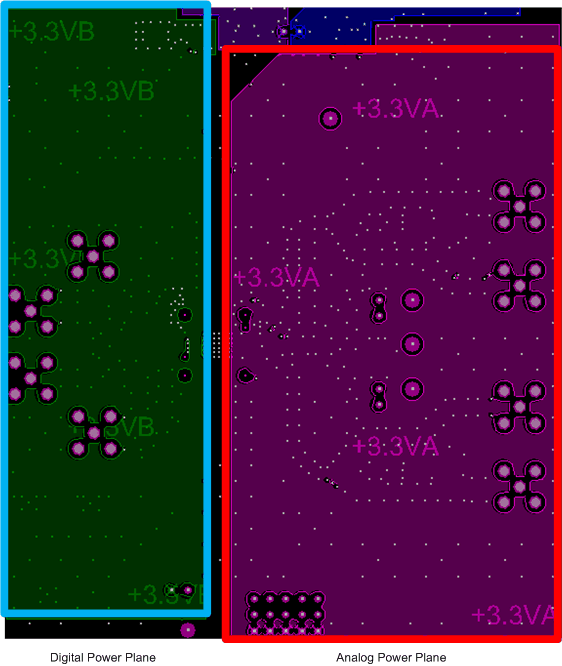 Figure 11-3 Power Plane (Layer 3)
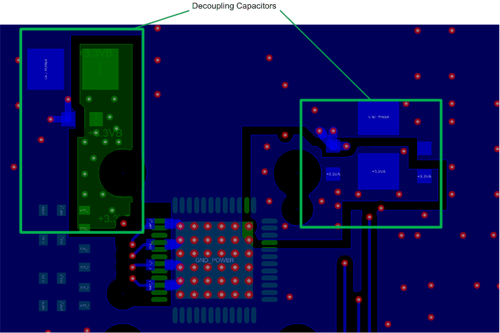 Figure 11-4 Bottom Layer (Layer 4)
 Figure 11-1 Top Layer (Layer 1)
 Figure 11-2 Single Ground Plane (Layer
2)
 Figure 11-3 Power Plane (Layer 3)
 Figure 11-4 Bottom Layer (Layer 4)