JAJSJI2D July 2004 – October 2021 DAC5662
PRODUCTION DATA
- 1 特長
- 2 アプリケーション
- 3 概要
- 4 Revision History
- 5 Pin Configurations and Functions
-
6 Specifications
- 6.1 Absolute Maximum Ratings
- 6.2 ESD Ratings
- 6.3 Recommended Operating Conditions
- 6.4 Thermal Resistance Characteristics
- 6.5 Electrical Characteristics
- 6.6 Electrical Characteristics
- 6.7 Electrical Characteristics, AC
- 6.8 Electrical Characteristics, DC
- 6.9 Switching Characteristics
- 6.10 Typical Characteristics
- 7 Parameter Measurement Information
- 8 Detailed Description
- 9 Application and Implementation
- 10Power Supply Recommendations
- 11Layout
- 12Device and Documentation Support
パッケージ・オプション
デバイスごとのパッケージ図は、PDF版データシートをご参照ください。
メカニカル・データ(パッケージ|ピン)
- PFB|48
サーマルパッド・メカニカル・データ
- PFB|48
発注情報
8.3.3 Differential With Transformer
Using an RF transformer provides a convenient way of converting the differential output signal into a single-ended signal while achieving excellent dynamic performance. The appropriate transformer should be carefully selected based on the output frequency spectrum and impedance requirements.
The differential transformer configuration has the benefit of significantly reducing common-mode signals, thus improving the dynamic performance over a wide range of frequencies. Furthermore, by selecting a suitable impedance ratio (winding ratio) the transformer can be used to provide optimum impedance matching while controlling the compliance voltage for the converter outputs.
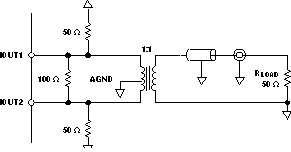
Figure 8-2 and Figure 8-3 show 50-Ω doubly terminated transformer configurations with 1:1 and 4:1 impedance ratios, respectively. Note that the center tap of the primary input of the transformer has to be grounded to enable a dc-current flow. Applying a 20-mA full-scale output current would lead to a 0.5-VPP output for a 1:1 transformer and a 1-VPP output for a 4:1 transformer. In general, the 1:1 transformer configuration will have slightly better output distortion, but the 4:1 transformer will have 6 dB higher output power.
 Figure 8-2 Driving a Doubly Terminated 50-Ω Cable Using a 1:1 Impedance Ratio Transformer
 Figure 8-3 Driving a Doubly Terminated 50-Ω Cable Using a 4:1 Impedance Ratio Transformer