JAJSGY9C february   2019  – july 2023 DLP2010

PRODUCTION DATA  

  1.   1
  2. 特長
  3. アプリケーション
  4. 概要
  5. Revision History
  6. Pin Configuration and Functions
  7. Specifications
    1. 6.1  Absolute Maximum Ratings
    2. 6.2  Storage Conditions
    3. 6.3  ESD Ratings
    4. 6.4  Recommended Operating Conditions
    5. 6.5  Thermal Information
    6. 6.6  Electrical Characteristics
    7. 6.7  Timing Requirements
    8. 6.8  Switching Characteristics
    9. 6.9  System Mounting Interface Loads
    10. 6.10 Physical Characteristics of the Micromirror Array
    11. 6.11 Micromirror Array Optical Characteristics
    12. 6.12 Window Characteristics
    13. 6.13 Chipset Component Usage Specification
    14. 6.14 Software Requirements
  8. Detailed Description
    1. 7.1 Overview
    2. 7.2 Functional Block Diagram
    3. 7.3 Feature Description
      1. 7.3.1 Power Interface
      2. 7.3.2 Low-Speed Interface
      3. 7.3.3 High-Speed Interface
      4. 7.3.4 Timing
    4. 7.4 Device Functional Modes
    5. 7.5 Optical Interface and System Image Quality Considerations
      1. 7.5.1 Optical Interface and System Image Quality
        1. 7.5.1.1 Numerical Aperture and Stray Light Control
        2. 7.5.1.2 Pupil Match
        3. 7.5.1.3 Illumination Overfill
    6. 7.6 Micromirror Array Temperature Calculation
    7. 7.7 Micromirror Power Density Calculation
    8. 7.8 Micromirror Landed-On/Landed-Off Duty Cycle
      1. 7.8.1 Definition of Micromirror Landed-On and Landed-Off Duty Cycle
      2. 7.8.2 Landed Duty Cycle and Useful Life of the DMD
      3. 7.8.3 Landed Duty Cycle and Operational DMD Temperature
      4. 7.8.4 Estimating the Long-Term Average Landed Duty Cycle of a Product or Application
  9. Application and Implementation
    1. 8.1 Application Information
    2. 8.2 Typical Application
      1. 8.2.1 Design Requirements
      2. 8.2.2 Detailed Design Procedure
      3. 8.2.3 Application Curve
  10. Power Supply Recommendations
    1. 9.1 DMD Power Supply Power-Up Procedure
    2. 9.2 DMD Power Supply Power-Down Procedure
    3. 9.3 Power Supply Sequencing Requirements
  11. 10Layout
    1. 10.1 Layout Guidelines
    2. 10.2 Layout Example
  12. 11Device and Documentation Support
    1. 11.1 Device Support
      1. 11.1.1 サード・パーティ製品に関する免責事項
      2. 11.1.2 Device Nomenclature
      3. 11.1.3 Device Markings
    2. 11.2 Related Links
    3. 11.3 ドキュメントの更新通知を受け取る方法
    4. 11.4 サポート・リソース
    5. 11.5 Trademarks
    6. 11.6 静電気放電に関する注意事項
    7. 11.7 用語集
  13. 12Mechanical, Packaging, and Orderable Information

パッケージ・オプション

メカニカル・データ(パッケージ|ピン)
サーマルパッド・メカニカル・データ
発注情報

Typical Application

This section describes a pico-projector using a DLP chipset that includes a DLP2010 DMD, DLPC3430 or DLPC3435 controller and DLPA200x/DLPA3000 PMIC/LED driver. The DLPC3430 or DLPC3435 controller does the digital image processing, the DLPA200x/DLPA3000 provides the needed analog functions for the projector, and DMD is the display device for producing the projected image.

The DLPC3430 controller in the pico-projector embedded module typically receives images/video from a host processor within the product. DLPC3430 controller then drives the DMD synchronized with the R, G, B LEDs in the optical engine to display the image/video as output of the optical engine.
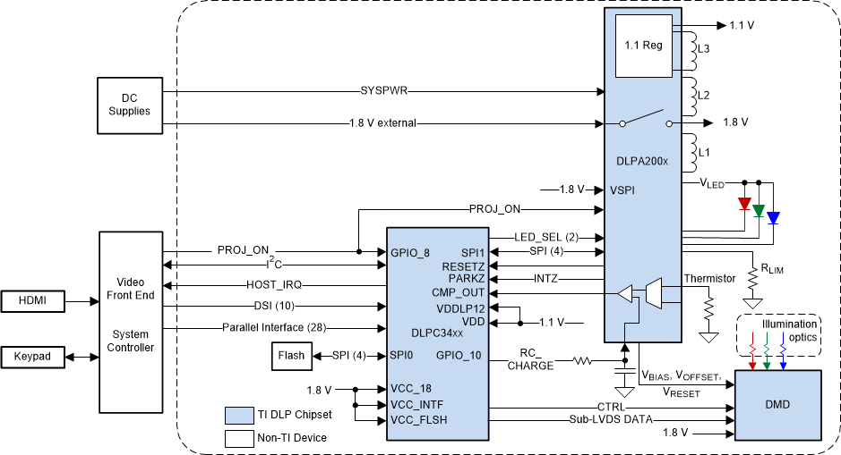
GUID-45BEB62C-CDD1-46E5-A840-901EE452B5EA-low.gif Figure 8-1 Typical Application