JAJSF42C April 2018 – December 2020 DLPC3478
PRODUCTION DATA
- 1 特長
- 2 アプリケーション
- 3 概要
- 4 Revision History
- 5 Pin Configuration and Functions
-
6 Specifications
- 6.1 Absolute Maximum Ratings
- 6.2 ESD Ratings
- 6.3 Recommended Operating Conditions
- 6.4 Thermal Information
- 6.5 Power Electrical Characteristics
- 6.6 Pin Electrical Characteristics
- 6.7 Internal Pullup and Pulldown Electrical Characteristics
- 6.8 DMD Sub-LVDS Interface Electrical Characteristics
- 6.9 DMD Low-Speed Interface Electrical Characteristics
- 6.10 System Oscillator Timing Requirements
- 6.11 Power Supply and Reset Timing Requirements
- 6.12 Parallel Interface Frame Timing Requirements
- 6.13 Parallel Interface General Timing Requirements
- 6.14 BT656 Interface General Timing Requirements
- 6.15 Flash Interface Timing Requirements
- 6.16 Other Timing Requirements
- 6.17 DMD Sub-LVDS Interface Switching Characteristics
- 6.18 DMD Parking Switching Characteristics
- 6.19 Chipset Component Usage Specification
-
7 Detailed Description
- 7.1 Overview
- 7.2 Functional Block Diagram
- 7.3 Feature Description
- 7.4 Device Functional Modes
- 7.5 Programming
- 8 Application and Implementation
- 9 Power Supply Recommendations
- 10Layout
- 11Device and Documentation Support
- 12Mechanical, Packaging, and Orderable Information
6.9 DMD Low-Speed Interface Electrical Characteristics
over operating free-air temperature range (unless otherwise noted)
| PARAMETER(3) | TEST CONDITIONS | MIN | TYP | MAX | UNIT | |
|---|---|---|---|---|---|---|
| VOH(DC) | DC output high voltage for DMD_LS_WDATA and DMD_LS_CLK | 0.7 × VCC18 | V | |||
| VOL(DC) | DC output low voltage for DMD_LS_WDATA and DMD_LS_CLK | 0.3 × VCC18 | V | |||
| VOH(AC)(1) | AC output high voltage for DMD_LS_WDATA and DMD_LS_CLK | 0.8 × VCC18 | VCC18 + 0.5 | V | ||
| VOL(AC)(2) | AC output low voltage for DMD_LS_WDATA and DMD_LS_CLK | -0.5 | 0.2 × VCC18 | V | ||
| Slew rate | DMD_LS_WDATA and DMD_LS_CLK | VOL(DC) to VOH(AC) for rising edge and VOH(DC) to VOL(AC) for rising edge | 1.0 | 3.0 | V/ns | |
| DMD_DEN_ARSTZ | VOL(AC) to VOH(AC) for rising edge | 0.25 | ||||
| DMD_LS_RDATA | 0.5 | |||||
(1) VOH(AC) maximum applies to overshoot. When the
DMD_LS_WDATA and DMD_LS_CLK lines include a proper 43-Ω series termination
resistor, the DMD operates within the LPSDR input AC specifications.
(2) VOL(AC) minimum applies to undershoot. When the
DMD_LS_WDATA and DMD_LS_CLK lines include a proper 43-Ω series termination
resistor, the DMD operates within the LPSDR input AC specifications.
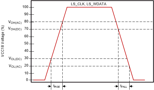
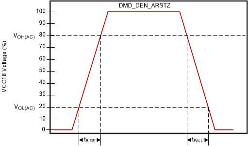
(3) See Figure 6-3 for DMD_LS_CLK, and DMD_LS_WDATA rise and fall times. See Figure 6-4 for DMD_DEN_ARSTZ rise and fall times.
 Figure 6-3 LS_CLK and LS_WDATA Slew
Rate
 Figure 6-4 DMD_DEN_ARSTZ Slew
Rate