SLVSBG3C June 2012 – June 2016 DRV120
PRODUCTION DATA.
- 1 Features
- 2 Applications
- 3 Description
- 4 Revision History
- 5 Pin Configuration and Functions
- 6 Specifications
- 7 Detailed Description
- 8 Application and Implementation
- 9 Power Supply Recommendations
- 10Layout
- 11Device and Documentation Support
- 12Mechanical, Packaging, and Orderable Information
パッケージ・オプション
メカニカル・データ(パッケージ|ピン)
サーマルパッド・メカニカル・データ
発注情報
5 Pin Configuration and Functions
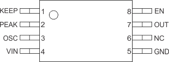
PW Package
8-Pin TSSOP
Top View

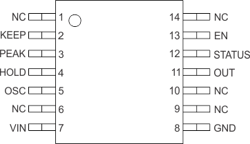
PW Package
14-Pin TSSOP
Top View

Pin Functions
| PIN | I/O | DESCRIPTION | ||
|---|---|---|---|---|
| NAME | NO. | |||
| 8-PIN PW(1) | 14-PIN PW | |||
| EN | 8 | 13 | I | Enable |
| GND | 5 | 8 | — | Ground |
| HOLD | - | 4 | I | Hold current set |
| KEEP | 1 | 2 | I | Keep time set |
| NC | 6 | 1, 6, 9, 10, 14 | — | No connect |
| OSC | 3 | 5 | I | PWM frequency set |
| OUT | 7 | 11 | O | Controlled current sink |
| PEAK | 2 | 3 | I | Peak current set |
| STATUS | - | 12 | O | Open-drain fault indicator |
| VIN | 4 | 7 | I | 6-V to 28-V supply |
(1) In the 8-pin package, the HOLD pin is not bonded out. For this package, the HOLD mode is configured to default (internal) settings.