JAJSCC6A June 2016 – July 2016 DRV2511-Q1
PRODUCTION DATA.
- 1 特長
- 2 アプリケーション
- 3 概要
- 4 改訂履歴
- 5 Pin Configuration and Functions
- 6 Specifications
- 7 Detailed Description
- 8 Application and Implementation
- 9 Power Supply Recommendations
- 10Layout
- 11デバイスおよびドキュメントのサポート
- 12メカニカル、パッケージ、および注文情報
パッケージ・オプション
メカニカル・データ(パッケージ|ピン)
- DAP|32
サーマルパッド・メカニカル・データ
- DAP|32
発注情報
6 Specifications
6.1 Absolute Maximum Ratings
over operating free-air temperature range (unless otherwise noted) (1)| MIN | MAX | UNIT | ||
|---|---|---|---|---|
| Supply voltage | PVDD, AVDD | –0.3 | 30 | V |
| Input voltage, VI | IN+, IN- | –0.3 | 6.3 | V |
| GAIN | –0.3 | VREG + 0.3 | ||
| EN | –0.3 | PVDD + 0.3 | ||
| Current | DC current on PVDD, GND, OUT+, OUT- | –8 | 8 | A |
| Operating free-air temperature, TA | –40 | 125 | °C | |
| Storage temperature range, Tstg | –50 | 150 | ||
(1) Stresses beyond those listed under Absolute Maximum Ratings may cause permanent damage to the device. These are stress ratings only, which do not imply functional operation of the device at these or any other conditions beyond those indicated under Recommended Operating Conditions. Exposure to absolute-maximum-rated conditions for extended periods may affect device reliability.
6.2 ESD Ratings
| MIN | MAX | UNIT | |||
|---|---|---|---|---|---|
| V(ESD) | Electrostatic discharge | Human body model (HBM), per ANSI/ESDA/JEDEC JS-001, all pins(1) | –2000 | 2000 | V |
| Charged device model (CDM), per JEDEC specification JESD22-C101, all pins(2) | –450 | 450 | |||
(1) JEDEC document JEP155 states that 500-V HBM allows safe manufacturing with a standard ESD control process.
(2) JEDEC document JEP157 states that 250-V CDM allows safe manufacturing with a standard ESD control process.
6.3 Recommended Operating Conditions
over operating free-air temperature range (unless otherwise noted)| MIN | NOM | MAX | UNIT | ||
|---|---|---|---|---|---|
| VDD | Supply voltage. PVDD, AVDD. | 4.5 | 26 | V | |
| VIH | High-level input voltage. STDBY, EN, FS0, FS1, FS2. | 2 | V | ||
| VIL | Low-level input voltage. STDBY, EN, FS0, FS1, FS2. | 0.8 | V | ||
| VOL | Low-level output voltage. INTZ, RPULL-UP = 100 kΩ, PVDD = 26 V. | 0.8 | V | ||
| IIH | High-level input current. STDBY, EN, FS0, FS1, FS2. (VI = 2 V, PVDD = 26 V). | 50 | µA | ||
| RL | Minimum load Impedance. | 1.65 | Ω | ||
| Lo | Output-filter Inductance. | 1 | µH | ||
6.4 Thermal Information
| THERMAL METRIC(1) | DRV2511-Q1 | UNIT | |
|---|---|---|---|
| DAP | |||
| 32 PINS | |||
| RθJA | Junction-to-ambient thermal resistance | 32.4 | °C/W |
| RθJC(top) | Junction-to-case (top) thermal resistance | 17.2 | °C/W |
| RθJB | Junction-to-board thermal resistance | 17.3 | °C/W |
| ψJT | Junction-to-top characterization parameter | 0.4 | °C/W |
| ψJB | Junction-to-board characterization parameter | 17.2 | °C/W |
| RθJC(bot) | Junction-to-case (bottom) thermal resistance | 1 | °C/W |
(1) For more information about traditional and new thermal metrics, see the Semiconductor and IC Package Thermal Metrics application report, SPRA953.
6.5 Electrical Characteristics
TA = 25°C, AVCC = PVDD = 12 V, RL = 5 Ω (unless otherwise noted)| PARAMETER | TEST CONDITIONS | MIN | TYP | MAX | UNIT | ||
|---|---|---|---|---|---|---|---|
| | VOS | | Output offset voltage (measured differentially) | VI = 0 V, Gain = 36 dB | 1.5 | 15 | mV | ||
| IVDD | Quiescent supply current | No load or filter | 20 | mA | |||
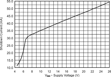
| IVDD(SD) | Quiescent supply current in shutdown mode | No load or filter | 35 | µA | |||
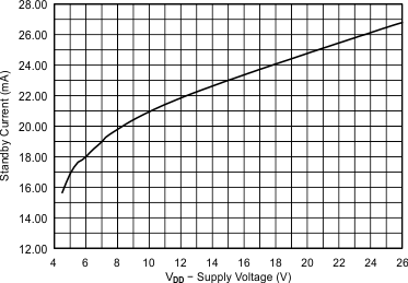
| IVDD(STDBY) | Quiescent supply current in standby mode | No load or filter | 11 | mA | |||
| rDS(on) | Drain-source on-state resistance, measured pin to pin | TJ = 25°C | 60 | mΩ | |||
| G | Gain | R1 = open, R2 = 20 kΩ | 19 | 20 | 21 | dB | |
| R1 = 100 kΩ, R2 = 20 kΩ | 25 | 26 | 27 | ||||
| R1 = 100 kΩ, R2 = 39 kΩ | 31 | 32 | 33 | dB | |||
| R1 = 75 kΩ, R2 = 47 kΩ | 35 | 36 | 37 | ||||
| VREG | Regulator voltage | 6.4 | 6.9 | 7.4 | V | ||
| BW | Full Power Bandwidth | 60 | kHz | ||||
| VO | Output voltage (measured differentially) | Measured at PVDD = 26V | 50 | V | |||
| PSRR | Power supply ripple rejection | 200 mVpp ripple at 1 kHz, Gain = 20 dB | –70 | dB | |||
| CMRR | Common-mode rejection ratio | –56 | dB | ||||
| fOSC | Oscillator frequency (with PWM duty cycle < 96%) |
FS2 = 0, FS1 = 0, FS0 = 0 | 376 | 400 | 424 | kHz | |
| FS2 = 0, FS1 = 0, FS0 = 1 | 470 | 500 | 530 | ||||
| FS2 = 0, FS1 = 1, FS0 = 0 | 564 | 600 | 636 | ||||
| FS2 = 0, FS1 = 1, FS0 = 1 | 940 | 1000 | 1060 | ||||
| FS2 = 1, FS1 = 0, FS0 = 0 | 1128 | 1200 | 1278 | ||||
| Power-on threshold | 4.1 | V | |||||
| Power-off threshold | 28 | V | |||||
| Thermal trip point | 150 | °C | |||||
| Thermal hysteresis | 15 | °C | |||||
| Over-current trip point | 13 | A | |||||
| Over-voltage trip point | 28 | V | |||||
6.6 Switching Characteristics
over operating free-air temperature range (unless otherwise noted)| PARAMETER | TEST CONDITIONS | MIN | TYP | MAX | UNIT | |
|---|---|---|---|---|---|---|
| ton-sd | Turn-on time from shutdown to waveform | EN = Low to High, STBY = Low | 10 | ms | ||
| tOFF-sd | Turn-off time | EN = High to Low | 5 | µs | ||
| ton-stdby | Turn-on time from standby to waveform | EN = High, STBY = High to Low | 6 | µs | ||
6.7 Typical Characteristics

